PCB Specifications: Don’t Over-Spec, Don’t Over-Pay By Al Wright, PCB Field Applications Engineer Epec Engineered Technologies
Among the most common questions Printed Circuit Board (PCB) suppliers receive are those dealing with production capabilities. Customers often worry that they are about to design in a feature which may be either at or outside of their fabricator’s limits. Fearing that their non-standard feature may add to the cost of their product, they inquire to find out just how much pain they are about to incur. In many cases the answer is that there is a straightforward way to do what’s needed without a lot of added cost. Other times, discussion reveals that the unusual requirement is either impossible, or nearly so. In these cases, additional work is necessary to identify a compromise allowing the order to go forward.
Too often, PCB designs get to the point where they are out for production bids before the customer discovers either that their project is going to be very costly or that nobody is willing to manufacture. This can become a panic situation, requiring a rushed redesign that sets back other work and leads to missed deadlines. The lost time can make it necessary to order prototypes on a rush basis at premium pricing.
This article will lay out some strategies by which PCB designers can develop an understanding of standard process limits and preferences for the typical board supplier, so they can better sense when they are about. This will make it possible to avoid over-specifying your PCB design so that you can achieve cost savings where possible.
Cost Control Begins Early
PCB designers often find themselves at odds with their purchasing and marketing departments after a design goes out for bids and comes back with a larger than expected price tag. Once the source of the high cost is identified, the questions fly:
- Why didn’t somebody see this coming?
- What happened that made the project so costly?
- When it seemed so straightforward?
- How does this affect our time to market?
- How do we recover?
Sometimes high cost originates at the project planning stage either because necessary research goes undone or the right people are not consulted. For example, if you have designed an apparently simple 2-layer board but it needs to accept a custom connector that requires a PCB of non-standard thickness, you have a problem. Either the PCB will require special-ordered base material or the PCB manufacturer will need to custom laminate the board as if it were a multilayer. Neither approach is ideal or free. Suddenly that ordinary looking simple 2-layer PCB will cost far more than it would have cost had the connector been designed around a commonly available PCB material thickness instead. A PCB which began life as an afterthought to the connector design team now turns out to be a major cost driver for the project.
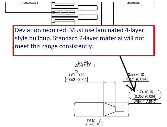 Figure 1: Connector designed without regard for standard material thickness. Special build required.
There are times where the need to use a single non-standard feature on the board itself may arise. Although it may seem insignificant at first, its presence could force the fabricator to add several process steps and to apply tighter process controls. These drive up the cost of what might otherwise have been a generic and inexpensive board.
It is best to get everybody together at the start of a project. Familiarize yourself with standard materials and practices before plunging ahead. If you have a design feature that you suspect may be out of the ordinary, talk to the people who will be manufacturing your product. It is in their interest to help you navigate around any potential problems before they find them on their own production floor. Try to understand which of your design choices is likely to add cost and then attempt to avoid those choices whenever you can.
Learn the Basics About Circuit Board Production
It is very important to have a grasp of the basic steps, tools, and materials that will be used to produce your circuit boards. Nothing will bring you up to speed more quickly than a tour through a manufacturing plant if it’s possible to arrange one. A working PCB manufacturer is the one place where you can view product at various stages of development as it moves from one station to the next.
You will see that a lot of the steps still involve a high degree of human oversight and interaction. You will gain an understanding of why it is always best to design your products as close to standard as you can, whenever it’s possible to do so.
If you cannot find a plant nearby, or if they are not able to provide a tour, check out some of the video presentations available online.
Aside from plant tours and online video it is useful to familiarize yourself with the standards published by IPC, the industry standards organization. IPC publishes comprehensive specifications, covering everything from design to final inspection. These specifications are not inexpensive but if you are committed to a career designing PCBs, consider investing in at least a digital copy of the design specification (2221 for rigid PCBs, 2223 for flex) and the acceptability standard (6012 for rigid, 6013 for flex). If you are working for a company that designs PCBs, they most likely they belong to IPC and may already own some or all the specifications.
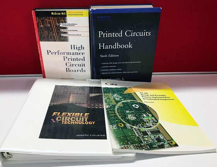 Figure 2: Assortment of publications related to PCB design and manufacturing.
Design Rules: Understanding What’s Standard
Having learned the basics of the production cycle you now need to understand where the limitations of your fabricator’s process life. If you’re using CAD software to generate your PCB files, you need to learn the design rules for the features you’ll use in your design so you can produce clean, buildable files.
Most fabricators maintain published design rules on their company’s web site. These cover rules for trace width, copper-to-copper spacing, minimum drillable hole diameter, maximum or preferred PCB outline size, etc. If you read a few of these, you will see that in most cases the values are very similar from one supplier to the next. You may also notice that many sites list multiple sets of rules because process limits are driven by your design’s copper weight.
Often you will find capabilities divided into two categories. One will be for “standard” rules, while the other will be designated “special” or “advanced.” Whenever possible use the standard set and configure your CAD program so that your layout does not stray outside these rules except in cases where there is no other way to meet your design intent. Use of advanced values when they are not required is a big cost driver and can even render your board unbuildable.
Pay attention to materials and tools as well. Find out what material products your supplier stocks and use them or write your material specification to match the properties of the products they use. Special order material is extremely costly, especially for prototypes and small volume production.
Learn the standard rules for operations like soldermask application, plating thicknesses, PCB thickness, and mechanical tolerances. Whenever possible simply default to IPC’s commercial standard (Class 2 / Commercial). Doing so will save you time that would otherwise be wasted making redundant callouts. Any qualified participant in the manufacturing process understands what the IPC standards say and how to meet them so calling out the spec is a form of shorthand upon which all of the participants can agree.
Understanding tools is also important. Small drill bits can reduce the efficiency of the drilling cycle. They are brittle and prone to breakage and cannot drill as deep as larger bits. They force the fabricator to reduce the number of panels that can be stacked together which increases cycle time and adds cost. Small routing tools have the same problems. Below a 0.062” bit, routing can become another bottleneck as long the cycles tie up machine time. Ask questions so that you can understand the points at which production becomes more difficult. See what your fabricator can suggest. Often there is another approach which will work for your product and will improve the fabricator’s yield.
Bottleneck Process Steps
Certain PCB manufacturing steps lend themselves to becoming bottlenecks where work is constantly stacking up and bogging down. There are several reasons why bottlenecks occur, and every manufacturer is a little different. Some may lack sufficient capacity in certain areas because of inadequate space or inability to justify having an extra machine on hand that will only run during peak periods. Others must outsource seldom-used processes on occasions when they are required. In general, certain processes lend themselves to bottlenecking, even when there are strategies in place to counter them. The ability to counter these production choke points at the design stage is limited. Sometimes you need the features you need, and little can be done to make them run faster. In such cases, your goal should be to avoid compounding the problem by creating other needless bottlenecks elsewhere in the manufacturing cycle.
Drilling is usually the earliest process that will bog down. With the prevalence of higher density surface mount designs, most of the holes on most designs are vias and some via drilling cycles run into the tens of thousands of hits. Vias use small, fragile, short-fluted drills. The fabricator would prefer larger drills that could penetrate multiple PCBs stacked on top of one another but the tiny via drills cannot go very deep and are prone to breaking.
Consequently, drill cycles are less efficient because fewer panels can be drilled at one time versus an equivalent quantity of larger holes. Rather than tie up general purpose CNC drill machines with vias, many fabricators now employ one or more dedicated multi-spindle machines that exclusively drill vias at very high rates of speed. While this helps somewhat, it only claws back a small portion of the increased time and cost.
As a designer you may sometimes have the option to use slightly larger vias such as 0.012” or 0.014” diameter in place of 0.008”. The fluted area of these bits is somewhat longer than it is on the smallest bits, the extra length may provide enough of a change that the panels will become stackable.
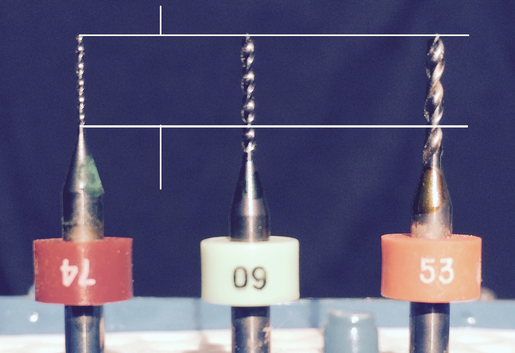 Figure 3: Example of shorter drill sizes used in manufacturing.
Another thing you can do to improve drilling efficiency is to consolidate tool sizes wherever possible. If you find that you have a drill file with 25 separate tool callouts only 0.001” or so different from the one next to them, look to combine some of them to get that machine’s spindles out of the air and back on the panel.
If you need to use blind and/or buried vias then these will add significantly to your cost. The boards will go through multiple lamination stages and may need to be drilled multiple times, often using expensive laser machines. When you need to use blind drilling and HDI with sequential lamination, it is sometimes possible to optimize your connections to eliminate one or more cycles.
When you have several sets of blind vias, review the design to see if there is another way to route the circuitry. If your board does not include high density circuitry and sophisticated BGA components, you may find that you can reduce the number of cycles which will bring your cost down. One clue is that you may have as many drill cycles as you have layers. In such cases, there are almost always methods for eliminating some or even all the extra drilling and lamination by re-thinking how the connections are formed.
Related to blind and buried drilling is the “Via-In-Pad” process. When it is necessary to utilize component pads as via locations it is usually also necessary to fill the vias with epoxy to prevent solder escaping through the hole at assembly. The epoxy needs to be planarized and plated over in a separate operation, so the pad can be reclaimed for soldering. The cost of your board increases but the savings in surface area is often worth the money. Nevertheless, any time you can avoid using via-in-pad processing, you will save money by finding other locations for the vias.
Plating is not generally a bottleneck, but it is more likely to become one if you specify something non-standard. Generally plating is straightforward -surface area times amount of plating equals plating equals cycle time. If your board requires thicker than normal copper, then it will require more time and may to some extent disrupt the normal process. Extra heavy or extreme copper plating is even more disruptive. It requires that the fabricator add capacity by installing extra and/or dedicated tanks to handle the many extra hours during which normal tanks would not be available for anything else to be plated. The best strategy with plating is to keep things as simple as possible while still meeting your design requirements. Follow IPC’s standard tables whenever possible.
Routing with small tools such as those used for key slots or small-radius cutouts, limits panel stack heights. This means that if a cycle is long, a single order may tie-up the machine for an inordinately long time. When such small features are unavoidable there is no easy answer (in other words, there is no equivalent to a dedicated via drilling machine to reduce the cycle time). However, you are not completely helpless. You can choose a faster cutting larger router bit such as .093” or .100” for the tab-routing of the outline to buy back some of the time. Or, if dimensional accuracy is not critical, you can choose to v-score the outline to get the job off the router entirely once the small critical items have been cut out.
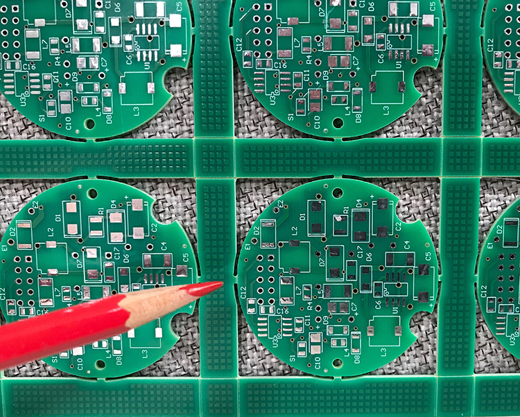 Figure 4: 0.031” routing path means 1 panel routed per cycle instead of 3. Inefficiency = cost.
Tight Tolerances and Cosmetics
Always try to remain within standard tolerance ranges when designing a board. Tighter than normal tolerances require more monitoring and more human interaction which results in more boards being scrapped for small nonconformances. If you have a press-fit hole size that must be controlled to +/-0.002”, that does not mean that you should apply that same tolerance to all the other holes in the design. Do you really care whether the 2,200 vias are within +/-0.002”, when they are all filled with soldermask anyway? Of course not. The same principle applies to outline dimensions (no tighter than +/-0.005”) and overall PCB thickness (typically +/-10%.) These tolerances became standard because they were achievable and repeatable. Unless you really need something tighter, stick to what’s normal. Your reward will be a normal price.
The same goes for cosmetics. If you cannot permit even the slightest cosmetic defects, then you will have great difficulty finding a supplier who will not charge a premium for all the perfectly functional boards they need to scrap on account of tiny touch-ups or other flaws. If your board is for everyday use apply everyday tolerances and pay everyday money.
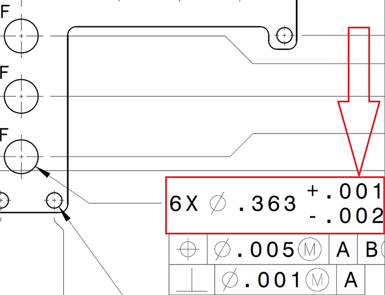 Figure 5: An almost impossibly tight tolerance applied to a routed plated through hole.
Reasonable Specs Equal Reasonable Prices
In today’s competitive business climate bringing your project in at a reasonable cost while meeting time-to-market goals is more important than ever. Designing your product for ease of production will give you your best shot at beating competitors to the punch. A steady and predictable delivery schedule makes it more difficult for similar products to gain a foothold. Use every available resource to understand how you can design your product to be as good as it can be without resorting to boutique manufacturing processes or needlessly stringent tolerances. Read, watch, and learn. Talk to your suppliers. Then hit the market confident that you will be able to respond to whatever demand arises.
Paying Too Much For Your Circuit Boards?
Maybe have our CAM engineers look at your design to see if we can reduce costs. Our team of experienced engineers is here to help you with all your circuit board needs from design, prototypes, and production.
Request a Quote Request Design Support


