Critical Manufacturing Process Steps of Rigid-Flex PCBs By Paul Tome, Product Manager Flex & Rigid-Flex Epec Engineered Technologies
Rigid-flex circuit boards and rigid printed circuit board (PCB) manufacturing have many of the same processes and use equipment that on the surface appear to be the same. There are however many significant differences in what the processes entail, how they’re performed, and how the equipment is configured between the two technologies.
The differences are driven by different materials and unique construction requirements which results in multiple rigid areas interconnected by flexible sections. In this article, we’ll discuss three of the more critical manufacturing process steps and how/why they differ from those used in traditional rigid PCB manufacturing.
Lamination Process
With rigid-flex PCB designs, the lamination process(s) is more involved than that of a rigid-only design. Maintaining registration between layers is critical to both technologies however a rigid-flex PCB has additional challenges in that there are polyimide flex layers, which do not have the same dimensional stability as rigid layers, and the pre-preg rigid area bonding layers (Figure 1a) are no longer solid sheets of material.
Pre-preg layers (Figure 1b) require the removal of material from the areas that will become the flexible sections of the design. This is done as a routing operation prior to lamination. The combination of these items results in a greater challenge in maintaining layer-to-layer registration.
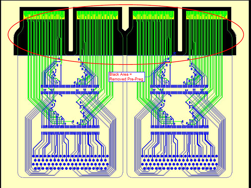 Figure 1a: Example of a pre-preg layer in a rigid-flex PCB design.
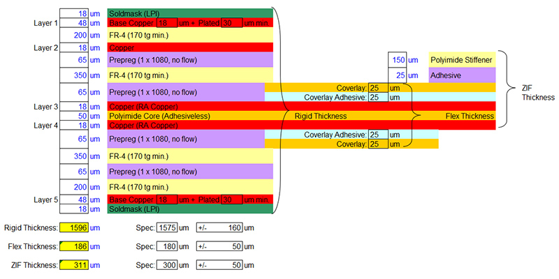 Figure 1b: Stack-up with pre-preg layers in a rigid-flex PCB design.
In addition, flex layers, prior to being laminated within the rigid layers, may require multiple additional lamination processes. All flex layers require sections of coverlay (Figure 2) to be attached, under heat and pressure, to encapsulate the flex area circuitry. Designs with three or more layers will need to have the flex layers laminated together. Some designs may also have stiffeners in the flex area(s), for ZIF contacts or supporting component areas, adding yet more lamination processes. Each lamination process creates the opportunity for the layer(s) to change dimensionally which then complicates maintaining layer-to-layer registration at the final lamination process.
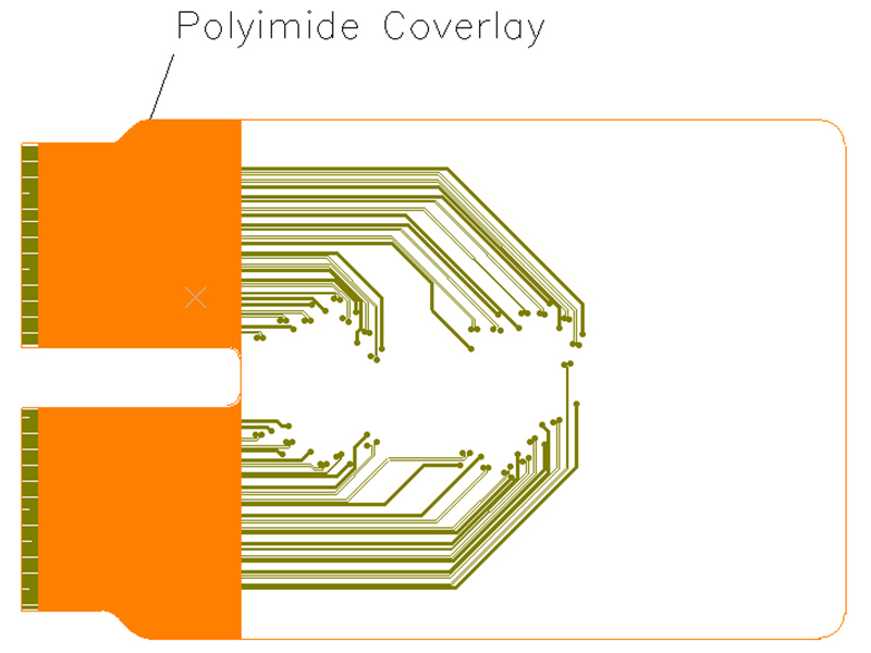 Figure 2: Internal flex layer with coverlay.
Both rigid and rigid-flex PCB designs require the individual rigid layers to be coated with a thin layer of adhesion-promoting brown oxide prior to lamination. The flex layers, in a rigid -flex PCB, require an additional plasma-based cleaning operation to ensure proper adhesion to the epoxy-based pre-preg layers that bond all the layers to one another.
Drilled Hole Cleaning & Preparation
The drilling operation is similar to both technologies in terms of the feeds and speeds used to drill the holes. What changes is the method in which the holes are cleaned and prepared prior to depositing the copper seed layer and the copper plating process.
This step is critical to achieving a properly plated hole in which the copper plating makes a full and robust interconnect to the internal circuit pads. The purpose of the cleaning process is to remove all epoxy smears from within the barrel of the drilled hole. This is a byproduct of the heat generated during drilling which melts the FR4’s epoxy resin and spreads it within the barrel of the hole. If not removed it becomes a barrier between the soon-to-be-plated copper and the internal pad connections resulting in poor reliability partial connections or complete open circuits.
Rigid PCBs use very aggressive chemical solutions to remove the epoxy smear. A rigid-flex PCB requires a plasma-based process to perform this operation. Chemical methods are too aggressive and uncontrollable for Polyimide flex core layers and would remove too much material.
A plasma etching system consists of a vacuum chamber within which the drilled production panels are racked. A gas is introduced into the chamber and energized to a plasma state with a high-frequency high voltage. The ionized plasma then dissolves the epoxy smear in a controlled manner. The process is adjusted by means of the gas used and the frequency of the high-voltage source.
Profiling
Creating the outline profile (Figure 3) for most rigid PCB designs is a straightforward mechanical routing operation without any significant complexities or tight tolerances. While this process applies to rigid-flex designs they also have additional critical profiling requirements. The polyimide flex layers require an outline cutting process however polyimide, due to its ductility, does not rout well. A routed flex edge is very ragged which can create mechanical stress concentrators which lead to the flex layer ripping.
 Figure 3: Example of a plated hole profile.
The preferred solution is to cut the flex area outline, prior to lamination, with either a laser or a precision punch and die set. Both methods provide a smooth edge finish. The standard tolerance is +/-0.005” however if the flex area has a ZIF connector the ZIF finger area requires a +/- 0.003” tolerance as per the connector supplier’ specifications.
Rigid-flex circuit boards also have a unique controlled depth routing operation required to remove the rigid layer materials from the required flex areas. This is a very precise operation as the clearance from the underside of an adjacent rigid layer to the coverlay encapsulated surface of the flex layers can be as little as 0.003” – 0.004”. The end of the router cannot be allowed to contact the flex layer as it would easily gouge into the flex coverlay and damage the parts. Figure 4a displays the production panel after lamination with the external FR4 layers extending throughout the individual parts and the production panel. Figure 4b is the construction once the individual parts have been control depth routed to remove the external layer FR4 from the flexible areas.
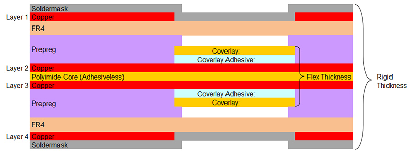 Figure 4a: Prior to FR4 removal in flex area.
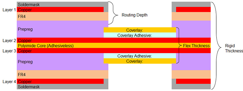 Figure 4b: After FR4 removal in flex area.
Summary
Rigid-flex PCB manufacturing includes all of the challenges of rigid circuit boards plus a significant number of additional requirements that are critical to the operation and reliability of the finished parts. These items are driven by the hybrid construction of rigid and flex materials that result in an integrated rigid-flex circuit that can be bent into a specific shape to meet the requirements of the final assembly.
On average a comparable layer count, a rigid-flex circuit board may have 50% or more process steps required to create the finished circuit as compared to a rigid circuit board. For the most part, the equipment and the process name are similar but there is a significant difference in the details of the process steps and how the equipment is configured and used.
Need Help With a Rigid-Flex PCB Design?
Our team of engineers can help you to design the most cost-effective and reliable rigid-flex circuit board, manufactured to the highest quality standards.
Request a Quote Request Design Support


