Advantages and Disadvantages of Thinner PCB Designs By Angie Brown, PCB Product Manager Epec Engineered Technologies
Printed circuit boards (PCBs) come in all sorts of shapes and sizes along with different technology levels. Some square or rectangular, round, or multiple cuts and angles are used as a pattern of design for the profile of the PCB. Usually, the shape will depend on the application of insertion as well as the internal cutouts. But what about the thickness or thinness of the part? How does that play a role in the manufacturing process, or does it matter?
PCB Callouts
In general, most of the time, the typical PCB is 0.062” thick, plus or minus the 10%, allowed per the IPC current revision level. That sounds simple enough. It is a standard that is not so standard to meet in many cases, and more often than not, it could require some consideration.
We use the 10% rule to calculate the finished thickness. When we talk about industry standards or IPC versus manufacturing capabilities, some of the time a callout cannot be met. Take an 0.062” +\-10% callout of a simple 2-layer circuit board. Many laminate manufacturers know that this is a common callout and manufacture 0.059” core materials knowing the standard can be met using 0.059” with the addition of plating and surface finish. Now, take the same 2-layer board and change the material finish to be 0.055” +\-10%. If the core standard is 0.059” to start out with, we are already 0.004” to the plus side of the final +0.0055”. This leaves no room for manufacturing finish. This, combined with stock limits, can push you to “special” made material at a high cost.
Taking the same thickness 0.055” and having a 4-layer part gives manufacturer's options to use different cores to meet the overall requirements. For example: 0.014”, 0.021”, 0.028”, and 0.031” are all common core thicknesses that could be used to manufacture this circuit board. When the thickness is much higher, however, you will run into some issues.
In Figure 1 for example, this is a PCB with 2X the thickness of most parts that we manufacture. The 0.125” thickness can add cost due to items such as additional prepreg, fewer panels that can be processed at a single pass in drilling and routing, and heavier weight.
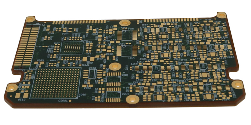 Figure 1: Thicker PCBs can lead to additional costs during manufacturing.
Overall PCB Thicknesses
The overall thickness is compiled using materials, plating, and surface finish typically. The thickness or thinness desired plus the tolerance, in most cases, is all that is supplied to manufacturing. Thicknesses are calculated by production when not specified by customers using standard balanced construction considering the overall.
The same is true for thin circuit boards. For example, 0.062” is standard, or typical for 4-, 6-, 8-, and even 10-layer circuit boards. Adjustments are made to core and prepreg thicknesses to meet the overall but what if you change the overall to 0.050” or 0.031”? The answer is, pushing the thickness to thinner also impacts the stack-up and overall 10% rule (the thinner the part, the less room manufacturing has for final tolerance to be met adding cost to the build).
In one instance, the same 4-layer board at 0.031” thick would use a different core material such as 0.014” instead of 0.028” for a 0.062” thick part as well as thinned dielectrics to meet the total thickness. The change to the thickness of the part still uses the same IPC rule of +\-10% overall, however, the overall is now +\-0.0031” instead of 0.0062”, 50% less. The more layers added to a PCB, the less play you have on material choices and the more difficult it can be to process.
These 3 stack-up images (Figure 2) are all for 4-layer PCBs. They all contain 1oz copper for the layers, however, different dielectric thicknesses are needed for each one to meet the overall requirements for final thickness. Increasing the core dielectric allows for cost-savings in prepreg sheets maintaining the same quality product.

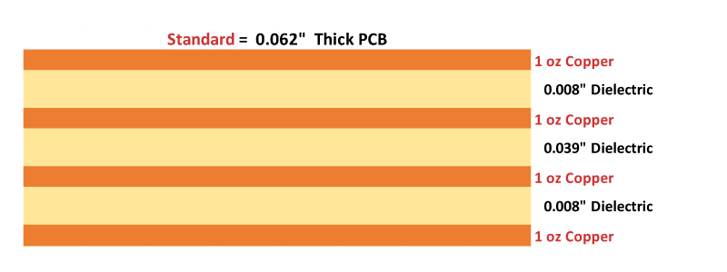
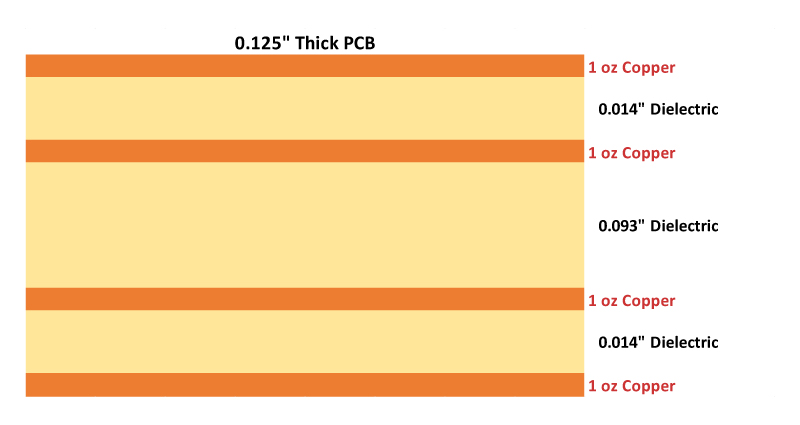 Figure 2: A 4-layer PCB with 1oz copper for the layers increases in thickness when increasing the core dielectric.
How Thin is Too Thin For A Circuit Board?
Well, the answer to that depends on several factors that must be considered. The overall copper weight for inner layers, dielectrics to prevent noise or crosstalk, impedance values, and the stack-up total thickness.
Thinner cores are more difficult to process through equipment and handling alone can cause damage to the core. The more layers involved in the build of the part, the more cost to the PCB. As you add layers to the circuit board it is typical to decrease the core thickness and prepreg filler gaps, however, there are limitations that cannot be crossed.
When designing the PCB, consider the final application, how much room you have for the PCB, and the size of the area for the part to fit. Using 0.062” is a base thickness to start with and tweaking that thickness up or down is best. Increasing the thickness can add cost, while decreasing the thickness can increase the risk of fallout, therefore, increasing the cost.
A 2-layer thinner PCB is 0.31” thick, half the normal standard thickness of 0.062”. As you can see (Figure 3), circuitry is visible from the top side for the bottom layer. The moon figure is not only more difficult to route due to the shape, but being thinner the program must be carefully planned to maintain tolerances for the radius, form fit, and function.
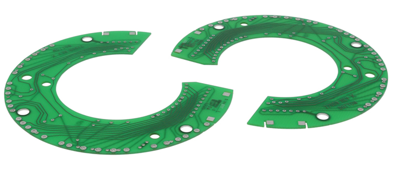 Figure 3: An example of a thinner PCB at 0.31” thickness.
Advantages and Disadvantages
With thinner PCB designs come pros and cons. Some of the advantages include:
- Reduced size and weight: Thinner PCB designs reduce the overall weight of the device, making it easier to transport at a lower cost.
- Improved circuit performance: Thinner designs allow for improved impedance controls with higher frequencies performance due to the reduced trace and layer thicknesses. This can result in shorter routing times and improved signal integrity.
On the other hand, some of the disadvantages are:
- Increased risk of damage: Thinner PCB designs are more prone to physical damage due to their reduced stiffness and strength. This can make them more vulnerable to bending, cracking, and other types of mechanical damage including manual handling in production.
- Increased risk of thermal issues: Thinner PCB designs can also be more prone to thermal issues due to their reduced thermal mass. This can lead to overheating and premature failure of components, or even the entire board.
- Increased risk of solder joint issues: Thin PCBs can also be more prone to solder joint issues due to their reduced area for soldering. This can lead to poor connections, cold solder joints, and other types of electrical issues.
- Reduced signal integrity: Thinner PCBs can also suffer from reduced signal integrity due to their reduced area for routing. This can lead to increased crosstalk and signal loss, resulting in reduced performance.
- Fragility: Thin PCBs are more fragile and can easily break or crack, especially during handling or assembly. This can lead to increased manufacturing costs and a higher rate of defective products as fabricators require additional steps to manage very thin PCBs.
Summary
Thinner PCB designs often come with advantages such as cost savings and more space for other components, but also have some drawbacks such as difficult production and handling, decreased copper weight in inner layers, and a greater risk of noise and crosstalk. Consulting with a PCB supplier or engineering staff early on in the process can help make sure you get the best possible design for your needs while avoiding any potential pitfalls.
Consulting your supplier and engineering staff for stack-up assistance can be advantageous early on to help you decide what would work best for both companies. Epec has a free online design for manufacturability (DFM) service monitored by our trained engineering team members so that they can guide you to a successful build of your PCBs.
Not Sure What PCB Thickness You Needed?
Our team of experienced engineers is here to help you design and manufacture a high-quality circuit board solution to get you ready to move into production.
Request a Quote Request Design Support


