Engineering Yourself Into a Corner With a PCB Design By Angie Brown, PCB Product Manager Epec Engineered Technologies
As a manufacturer of printed circuit boards, we see many different flavors of PCBs. The complexity of a printed circuit board has changed greatly over the years. In this article, we will discuss the top design issues we see repeatedly that cause process challenges, scrap, and fallout.
Data Review
During pre-production design review, engineering will use a preset parameter for automated inspection. Prior to inspection beginning all the circuit board layers are checked for alignment to each other and to the supplied drill and non-plated drill. Verification of a 1-to-1 outline is also needed for measurement, data to datum checks, and copper checks.
Often a 1:1 Gerber file outline is not supplied and must be created by engineering or copied from a layer if there is one supplied on the Gerber layers. A complete dimensioned drawing or fabrication drawing is key to programming and design for manufacturing checks. A Gerber outline should be exact to the desired PCB profile. It should include a hole to board edge dimension X, Y a hole chart, any cutout features, or slots. Every parameter checked in preproduction CAM somehow relates back to the outline.
You can see (Figure 1) the importance of having a 1:1 Gerber file outline. This PCB has many cuts creating the profile, without a supplied outline and a dimensional drawing it would be difficult to interpret what the actual should be. We can measure and create a routing profile from the 1:1 Gerber file. When we receive a PDF or other Word document and no Gerber file with an outline, the outline layer must be created from the drawing; it must exactly match the desired shape. Creating an outline that is not supplied leaves room for human error.
The outline should be drawn with a line of any width starting at 0, 0. The line should be exact in all X, Y coordinated and dimensioned for verification. We often find critical errors where the numeric dimension does not match the outline. All dimensions are verified within the CAD tool. Determining the drill location start position within the outline for one. All holes are based off an X and a Y coordinate and consecutive coordinate from that first drilled location to the next.
Etch Factor
Placement of data in relation to the board edge is critical to processing challenges. Copper features to board edges should be considered. When a circuit board is routed the minimum distance of any copper should be to the actual board edge is 0.010.”
During the routing process, the router bit travels along the edge of the PCB, rotating to cut the part from the panel. As in all equipment, parts, and manufacturing there is a tolerance needed. A +/-0.005” is standard processing tolerance for routing. Keeping metal 0.010” from the edges allows for standard processing.
Knowing the hole to board edge is critical to the routing or scoring program details, without this critical placement dimension it is unknown where the holes lie within the profile of the PCB. The actual hole is measured (Figure 2) to the 0, 0 to verify the location of the positioning of the drill program. Knowing this dimension is critical.
Pad-to-Hole Size
Copper features are critical to functionality of the product, impedance values, component placement and longevity of your device. Let’s discuss copper a little further in regard to layout or routing of the copper layers.
Copper to edge is a problem; any exposed copper will oxidize and is prone to shorting the PCB to components, casing, and final assembly. All copper is typically covered with solder mask or surface finish. When copper is exposed by end processing, either routing or scoring, this is after mask and surface finish leaving little option to correct. Mask touchup can be used, however, it is time-consuming and not appealing to the eye. For this reason, pulling copper back from the edge is important.
Copper to Edge
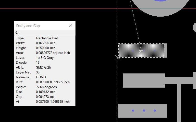
The copper features are 0.004” from the actual printed circuit board edge (Figure 3). Whether this part is routed or scored, after processing there will be exposed copper left behind on the PCB edge. To prevent exposed copper the pads will need to be resized, trimmed, shaved, from the edge 0.010” - 0.015” minimum.
 Figure 3: The copper features are 0.004” from the actual printed circuit board edge.
As we continue to push technology, line widths and spacing have decreased to common 0.005” and less. But what does this do to standard processing? Long gone are the standard 0.007” circuit and space. Materials are still most common at 1/2 OZ, 1 OZ and 2 OZ finish.
When the trace/space width is 0.005” the copper start weight should be a ½ OZ of copper. When etching a circuit board, the loss is typically 0.001” in feature size on ½ OZ copper, all circuitry is modified to allow for this loss however when the spacing will not allow for etching factor, the loss cannot be helped. Keeping etch factors in mind during the design and layout process will aide your PCB manufacturer to produce the part without greater loss in line width.
The increase in copper weight will increase the circuit loss in height and width as the chemical etches through the copper to the resin base surface. Whether it is circuit to circuit or pad or copper features considering the process is best to allow for quality production process.
BGAs, QFPs, components, resistors all have the same copper considerations needed as mentioned previously. As footprints continue to shrink, it is most common now for manufacturing hands to be tied in processing limitations. As we shrink below 5/5 for space, we see many components being designed and used with the same considerations as circuits. A BGA, for instance, can have 0.005” spaces with circuitry of 0.004” and neck downs to 0.003” and a call out of 1 OZ base copper. The copper weight is too heavy for the small width of the trace and the depth of the copper.
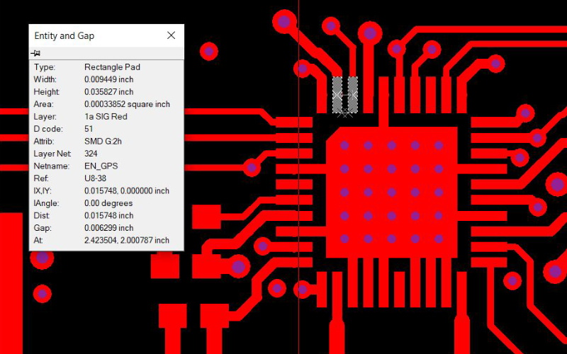
Starting with a ½ OZ base is doable but again difficult with the limitations built into the design. The gap is 0.006299” between copper pads (Figure 4): this space is too small to allow for etch factor increase; pad dimension loss could be problematic at assembly.
 Figure 4: The gap is 0.006299” between copper pads.
Another item to consider when choosing a component is the space between the leads. Typically, a 0.008” minimum space is needed to adhere soldermask to the surface of the laminate and to clear the mask off the copper pads. A typical mask clearance of 0.004” larger than the copper pad is needed to pull the mask off the pad surface. A 0.004” space from mask pad to mask pad is needed to adhere the mask to the laminate surface, we call this a web of mask. Less than 0.004” is difficult to process, the mask will lift and peel as well as flake and crack when sufficient spacing is not present.
When the copper-to-copper space is less than 0.008”, the risk of mask loss in areas where shorting is a concern is greater than normal. Removing the mask or gang masking the soldermask relief areas is recommended to prevent mask lifting and redepositing on to the part. Using GREEN mask as a standard processing color is also the preferred color over red, black, or white. The pigment in the mask color is also a factor unknown to most that has processing challenges related to mask adhering.
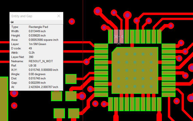
When the spacing is too small to adhere mask to the surface, gang masking is the best option to prevent issue with the soldermask lifting, cracking, and redepositing on the surface. Figure 5 shows a gap of 0.002299” from mask pad to mask pad, too narrow to allow for a web of mask to remain on the PCB. Webs of mask are critical to assembly in preventing solder shorts during processing.
 Figure 5: A gap of 0.002299” from mask pad to mask pad.
Summary
Designing yourself into a corner causes unnecessary problems for production of PCBs, PCB-assembly and your final product customers. Ask a PCB engineering member; the more you know during design and layout, the better. Epec provides a free DFM file check to help keep processing challenges, scrap, and costly prototyping to a minimum.
Need Help With A PCB Design?
Our team of experienced engineers is here to help you design and manufacture a high-quality circuit board solution to get you ready to move into production.
Request a Quote Request Design Support


