PCB Fine Lines and Spaces
High density interconnect (HDI) PCB technology, including fine lines and spaces (2 mil and below) is a key enabling technology for the next generation of portable electronic devices. This technology offers many advantages over conventional technologies, including circuit board size reduction, increased routing, and lower fabrication costs.
Today's trend in portable electronics is to manufacture smaller and lighter products with increased functionality. The size of the products we all use each day is only a fraction of the size it was a few years ago. Increased product functionality coupled with drastic size reduction places extreme demands on designers to increase silicon integration, reduce silicon packaging size, and reduce the printed circuit board size.
Advances in integrated circuit packaging technology, such as direct chip attach, ball grid arrays, and chip scale packages, have outpaced the ability of the printed circuit board industry to manufacture cost-effective motherboards on which to solder the packages.
Printed circuit board manufacturers must invest in specific equipment and technologies to be able to consistently produce circuit boards with 2 mil lines and spaces. This will be a small portion of the current PCB manufacturing resources today that are able to produce this type of product.
The cost to implement the required equipment to produce such product will be limited. As with every newer technology comes expense, overhead, and limited demand. Not every manufacturer will be able to justify the extreme costs for the lower demand.
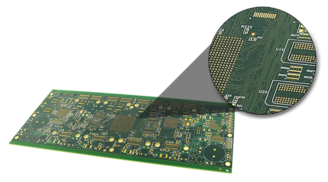
 Printed Circuit Board with Fine Lines and Spaces
PCB Processing for Imaging and Laser Direct Imaging
The PCB is prepped for film application by using a scrub, acid wash, and passed through air knives to dry the core or laminate. The clean dry surface of copper receives a dry film applied with heat and pressure passed through hot rolls. Different films are used for different imaging processes, technologies, and copper considerations, nonetheless a coating needed to image. The film is applied the same way whether it is for contact imaging or laser direct Imaging.
Laser Direct Imaging
For HDI printed circuit boards containing fine lines and spacing less than 0.004", laser direct imaging (LDI) is the best option. The imager uses a laser or LED to produce the image of the Gerber pattern directly onto the photoresist-coated panel. There is no film tool process involved in LDI. The Gerber tool is set up for production, and Gerber data is stepped, including any cross hatch, text, targets, or fiducials as required by processing. The PCB pattern is duplicated to maximize usage of the panel. It is then uploaded to the LDI for one side of the panel to be imaged into the resist.
The laser direct imager uses precise positioning of tooling holes or fiducial marks on the panel to properly image the panel. The LDI calculates very precise exposure definition to transpose the image of the Gerber to the film previously applied to the panel. LDI can be completed in 45-185 seconds or more per side compared to contact exposure which averages a 10-15-second exposure imaging both sides of the panel in a single exposure.
Contact film is reusable and requires storage space and has an annual cost depending on volume of $15k or more. Storage must be in a temperature- and humidity-controlled area, an addition added expense. Film can be dimensionally unstable causing registration issues in production. Film is prone to defects of scratches or particles that will cause shorting or opens if undetected. Adding to cost of repair or scrapping of product.
The PCB is prepped for film application by using a scrub, acid wash, and passed through air knives to dry the core or laminate. The clean dry surface of copper receives a dry film applied with heat and pressure passed through hot rolls. Different films are used for different imaging processes, technologies, and copper considerations, nonetheless a coating needed to image. The film is applied the same way whether it is for contact imaging or laser direct Imaging.
LDI does not require storage or film cost and should be in a controlled clean room, temperature- and humidity-controlled area. There is no risk to registration issue, and defects seldomly occur. Maintaining LDI, laser cost, replacement or repair can be $60k-$125k every 3-5 years.
Cupric Chloride Etching
Most PCB companies use the pattern plate/ strip/etch/tin strip process so ammoniacal etchant must be used due to the fact that cupric chloride will remove the tin or tin/nickel pattern plate applied as a resist along with all of the copper. However, cupric chloride etching is a much more controllable process and with very little effort and the most basic equipment, line, and space sizes down to 2 mil can easily be achieved using cupric chloride. Because of the significant cost of purchasing and maintaining 2 etching systems, most circuit board manufacturers only use ammoniacal etch for both fine lines and standard technology products.
Laser Drilling
With the need for fine lines and spaces comes the need for ultra-precise registration in the drilling process. With laser drilling and the automatic registration of the drilling pattern to optical targets (drilled or etched) is this drilling technology's main advantage. With the individual registration and the adaptation of the drilling pattern to the dimension of each circuit board, pad sizes could be reduced dramatically. Microvia target lands have a diameter between 300 μm and 250 μm, and they will continue to drop.
Without investing in the proper technologies, it is difficult for a PCB manufacturer to manufacturer fine line and space printed circuit boards down to 2 mils.
Have a PCB Design with Fine Lines and Traces?
Unlock the future of portable electronics with HDI PCB technology today for a cost-effective, high-performance solution that exceeds your needs.
Request a Quote Request Design Support Request More Information


