
Solder Mask Design Basics
Standards
Information on the use of solder mask is contained in IPC-SM-840C Qualification and Performance of Permanent Solder Mask. The specification is intended to facilitate evaluation of solder mask by a vendor using a standard board system, and to enable designer, manufacturer, and user together to qualify a production board process.
The test methods and conditions in IPC-SM-840C are based on end use and environmental reliability requirements for two classes1 of user:
1 Older IPC documents refer to Class 1, Class 2, and Class 3. For all practical purposes there is no Class 1 solder mask; Class 2 is equivalent to Class T; Class 3 is the equivalent of Class H.
T – Telecommunication (includes computers, telecommunication equipment, sophisticated business machines, instruments, and certain non-critical military applications.) Solder mask on boards in this class is suitable for high performance commercial and industrial products in which extended performance life is required, but for which interrupted service is not life-threatening.
H – High Reliability/Military (includes that equipment where continued performance is critical, equipment down-time cannot be tolerated and/or the equipment is a life support item). Solder mask on boards of this class is suitable for applications where high levels of assurance are required and uninterrupted service is essential.
IPC-SM-840C divides responsibilities between materials supplier, board fabricator and board user. The user's task is to "monitor the acceptability and functionality of the completed boards". Note particularly that IPC-SM-840C specifically does not "determine the compatibility of solder mask materials with post-soldering products and processes" – if you want to conformal coat the final product, it becomes your responsibility to check for compatibility.
Materials & Processes
When you discuss the materials and requirements for solder resist with your fabricator, you will have to take into account a number of factors:
- Class of application, T or H
- Physical size of the board
- Thickness of the conductors and the type of metallisation finish
- Track density on the surface, and how evenly spread the tracks are
- How many holes there are, of what size, and with what annular ring tolerance
- Whether components are placed on top of tracks
- Whether tented vias will be needed
- Whether the solder mask thickness will be important in defining the joint volume
The original solder mask was pattern-printed, using screen printing, but this technique has limitations on definition, with the result that photoimageable materials are used for most applications. As with any resist process, there is a choice between dry film materials, where a known thickness of mask is laid over the board, and liquid processes, where a deposit of approximately even thickness is attempted, typically in the case of solder resist by curtain coating.
You will appreciate from your study of Unit 2 that dry film materials adhere best to flat surfaces; given the necessarily uneven surface of the patterned board, a liquid photomask will be in more intimate contact with the foil and underlying laminate than a film type (Figure 1). For the highest definition, LPISM will generally be preferred, generally with a matte finish, because this reduces the potential of solder balling during reflow. For more information, check out our blog post on Circuit Board Solder Mask - What to Use and What Not to Use.
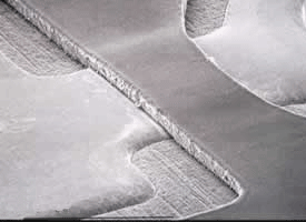
Figure 1: Example of dry film resist side walls
See our blog post titled Matte vs Gloss Solder Mask in Circuit Board Design for more information.
Layout Issues
Figure 2 shows in schematic a typical solder mask application. Notice the very definite three-dimensional nature of the board surface.
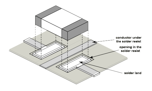
Figure 2: Solder resist on a printed wiring board
It is important that:
- The solder mask should be kept away from any plated through-hole and its associated land or pad
- Each conductor track should be covered
- The laminated area should be completely covered
- Adjacent conductors should not be exposed (not as Figure 3)
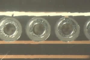
Figure 3: Exposed tracks due to over-size resist aperture
Solder mask artwork should be oversized to allow for misregistration or slump, which can obscure or contaminate a pad surface, causing excessive solder balls or defective joints.
We recommend that solder mask apertures should be approximately 150µm overall (75µm per side) larger than the pads, to prevent solder mask encroachment, and that a note should be added to the fabrication drawing stating that solder mask encroachment is not permitted on the component pins/pads, and allowing the board fabricator to modify solder mask apertures where necessary. In the same way, vias used as test points should be kept clear of encroaching solder mask on the side from which they are being probed.

Figure 4: A via tented with dry film resist
While vias may be covered by solder mask (referred to as "tented") (Figure 4), if vias are used as test points, care should be taken to have an aperture in the solder mask on the top surface, to allow gas to escape from the via during wave soldering. (Purves suggests that this should be 100µm larger than the finished drill size used for the via) This procedure allows the via to fill with solder and create a good test probe target.
Excessively thick solder mask can cause drawbridging where used between component pads, and omitting mask between chip component pads is sometimes recommended to reduce this effect, and also make cleaning easier. This of course is not possible when tracks are run in the spaces between pads. The two different types of solder mask window needed are shown in Figure 5, from which it is clear that pocket windows need solder mask that is much better defined and in register than gang windows.
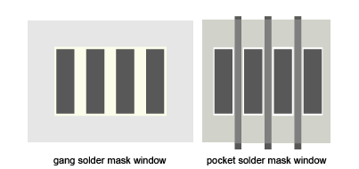
Figure 5: Solder mask window types
The gang solder mask window will normally be able to be manufactured by screen printing, using a 0.38 mm spacing; however, the pocket solder mask type will require clearances of 75–125 µm, and must therefore be made with photoimageable resist.
By the way, don't assume that putting fingers of resist between pads on an otherwise bare board might help overcome bridging, because most bridging occurs between component leads above the board. You are just adding to the cost by using a more expensive process, and gaining little.
IPC-2221 Generic Standard on Printed Board Design and IPC-SM-782 Surface Mount Design and Land Pattern Standard contain a number of recommendations and comments on other issues, some of which are summarized below:
- When solder resist is applied over tracks whose coating will melt when soldered (that is, not SMOBC), the tracks should be no more than 1.3 mm wide, or else have holes in them so that the coating can bond through to the underlying laminate
- The maximum finished hole size of tented vias should be 1.0 mm for both Class T and Class H
- Where tolerances are tight, as in the pocket solder mask case in Figure 5, consideration should be given to having more internal layers for routing connections, allowing the outer layers to be used only for solder lands. This approach is referred to as 'surface pads only' or 'pad cap'
Not Sure What Solder Mask Is Your Best Option?
Optimize your PCB design with IPC-SM-840C Standards. Ensure reliability & functionality for Class T or H applications. Here are some differences between coverlay and flexible solder masks.
Request a Quote Request Design Support Request More Information


