
Via Filling Process
The term via refers to a drilled hole that is copper-plated to create an electrical connection between two or more layers of a printed circuit board. Via filling is a PCB manufacturing technique in which the via hole is filled thereby completely closing the via hole using a conductive or non-conductive epoxy material or copper plating. Filling vias improves the reliability of the circuit board by decreasing the probability of trapped air or liquids in the via, which can cause failures during the assembly process, especially at the elevated temperatures that are required for today’s lead-free solders. For more background on this, read PCB Vias - Everything You Need To Know.
The most recent technological advancement in the via fill area is to utilize via-in-pad technology. While the via-in-pad process does increase cost versus the old-school “dog bone” method, there are significant benefits over conventional through-hole technology.
Micro-vias play a large part in the design HDI boards with smaller form factor and lower weight. Per IPC standards the definition of a microvia is a hole with a depth-to-diameter aspect ratio of 1:1 or less, and the hole depth not to exceed 0.25mm. Previously, microvia was loosely defined as any hole less than or equal to 0.15 mm in diameter. The lower form factor for microvias leads to a reduction in distances between components, which reduces the overall resistance of the traces resulting in better conductivity which is critical for breaking out connections for close pitch components such as BGAs.
Some key benefits of filled vias are:
- Tighter BGA pitches
- Increased thermal and electrical conductivity
- Reduced layer count or board size
- Improved routing density (higher density per layer)
- Strengthening pad attachment
- EMI reduction
- Gives high frequency designs the shortest possible route to bypass capacitors
- Overcomes high-speed design issues and constraints such as low inductance
There are three main options for via filling. Below we will review each of these options.
Conductive Via Filling
Conductive via filling allows the effective transfer of electrical signals from one side of the circuit board to the other, while enhancing its thermal transfer properties of the via. Conductive filled vias (copper or silver are the most common) are especially helpful for conducting a large amount of heat away from components as the metallic nature of the fill wicks heat away from the IC.
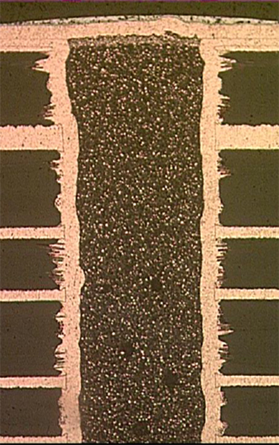 PCB cross section with conductive fill via.
Silver epoxy is more cost-effective and used more frequently but copper conductive epoxy is far better in terms of thermal conductivity. However, both will improve the quality of current conduction between the vias and the PCBs internal layers. It should be noted that conductive fill of vias is approximately 5x the cost of non-conductive fill.
Non-Conductive Via Filling
Non-conductive via fill is done using the same process as conductive except that it is usually done to prevent solder or other contaminants from entering the via rather than conducting heat and a signal. It also provides structural support for a copper pad covering the hole in the case of a via-in-pad. Keep in mind that the vias are still plated with copper so they will conduct heat and electrical signals, as the only difference between traditional vias is the air in the space is replaced by the fill material.
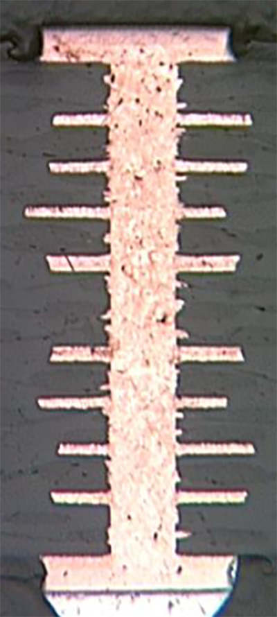 PCB cross section with non-conductive fill via.
It is always recommended to match the CTE values of the via filling to be used with the surrounding laminate to avoid future stress fractures due to contraction or expansion. Because the via fill material will heat up and expand far more rapidly than the laminate, this unequal expansion can cause a fracture to appear between the pad and the hole wall.
Copper-Plated Shut Filled Vias
Most PCB designers have experience with the use of filled vias using epoxy, but many are not familiar with the process of copper plated shut for either through vias and/or microvias, as not all PCB fabricators have invested in the proper equipment to perform this process.
Over the past several years, our NetVia Group facility in Dallas has developed a process that allows us to plate shut through-hole vias, up to 12 mils in diameter, without concern of voids, air pockets, or fluid entrapment in the holes. Without question, plated shut vias provide 10X the thermal conductivity of any other via fill solution, which makes it the most logical choice for thermal dissipation.
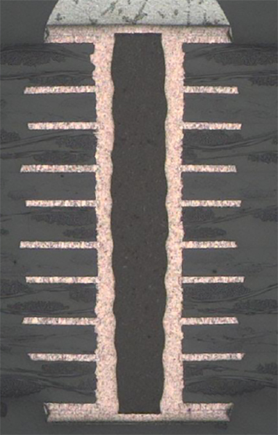 PCB cross section with copper-plated shut filled via.
Generally speaking, when the aspect ratio gets to 10:1 or via diameter is less than 8 mils, that is where we would opt to copper plate shut a via, but there are other specific attributes where it is very difficult to fill, or plate shut vias:
- Thin materials or subs (less than 20 mils) are more difficult to process through planarization as the material can tear and/or distort.
- If wrap plating is required, so terminating surfaces have a buildup of copper, making fine lines/spaces more difficult to process.
- PTFE/Teflon materials will dramatically distort.
Learn more about the Plated Shut Through Hole Vias process.
Need Help with PCB Vias?
Switch to via-in-pad technology for unmatched thermal conductivity and signal integrity. Request your free quote now to experience the future of PCB design.
Request a Quote Request Design Support Request More Information


