HDI Boards – High Density Interconnect
HDI circuit boards are a fast-growing PCB technology that uses blind and/or buried vias and often microvias to achieve higher circuitry density than traditional circuit boards. Epec offers HDI circuit boards and supports the design and manufacturing processes required for fine lines, tight spacing, and advanced via structures, including via-in-pad, laser drilling, and sequential lamination, so PCB designers can place more technology into smaller geometries without losing focus on quality.
See our blog post in regards to designing HDI PCBs.
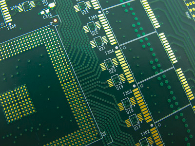
 Printed Circuit Board Using HDI Technology
At a Glance: HDI PCBs
- Higher density through advanced via structures: HDI circuit boards use blind and/or buried vias and often microvias to achieve significantly higher circuitry density than traditional PCBs, supporting smaller geometries and tighter component placement.
- Enables smaller, faster electronics: HDI technology allows designers to place more components on both sides of the PCB, increase I/O density, and reduce signal loss and delays as component size and pitch continue to shrink.
- Process-intensive but cost-conscious: While HDI manufacturing requires specialized processes such as laser drilling, via-in-pad, sequential lamination, and fine-feature imaging, thoughtful design can reduce layer count and material usage to offset added process cost.
Consumer Driven Technology
HDI circuit boards are now available at Epec and are among the fastest growing technologies in PCBs. HDI designs use blind and/or buried vias and often include microvias with very small diameters to increase routing density beyond traditional circuit boards. This shift is tied to long-term product trends where electronics have become physically smaller while expanding capability, quality, and speed.
The via-in-pad process is a key enabler for packing more technology into fewer layers, reinforcing the idea that higher capability does not always require larger form factors. Changes in consumer expectations and mobile computing have continued to push smaller, lighter designs that still need fast, reliable signal performance.
Key HDI Benefits
As component sizes and pitch decrease, HDI gives designers more options to use PCB surface area efficiently by placing more components on both sides of the raw PCB. Multiple via processes, including via-in-pad and blind via technology, help create more usable real estate for tighter component placement. Smaller geometries and increased I/O density support faster signal transmission and can reduce signal loss and crossing delays.
These benefits align with the evolution from earlier surface mount technology trends into higher-density packaging approaches that place more functionality into smaller square surface areas, while still requiring strong process control to maintain yield and consistency.
Via in Pad Process
The via-in-pad process allows vias to be placed within the surface of flat lands. In this process, the via is plated, filled with epoxy (conductive or non-conductive), then capped and plated over so it becomes nearly indistinguishable from the surrounding land. The outcome is a via structure that can be soldered like normal lands after the fill and cap steps are complete.
Although the result appears straightforward, this process adds significant complexity. There is an average of eight additional steps, and the work requires specialty equipment and trained technicians who closely follow the process to achieve consistent hidden vias.
Via Fill Types
HDI manufacturing uses multiple via fill approaches depending on the design and process requirements. Via fill options described for this process include non-conductive epoxy, conductive epoxy, copper-filled, silver-filled, and electrochemical plating. These approaches are used to create a via that is buried within a flat land so it can solder as a normal land.
Vias and microvias may be drilled as blind or buried structures, filled, then plated and hidden beneath SMT lands. Processing these vias requires specialized equipment and can be time consuming due to multiple drill cycles and controlled depth drilling that increase overall process time.
Cost Effective HDI PCBs
For many products, quality remains a primary requirement alongside price. HDI can help address both by enabling designs that reduce overall layer count while maintaining wiring capability. Using HDI technology during design, it can be possible to reduce an 8-layer through-hole PCB to a 4-layer HDI microvia technology packed PCB. A well-designed HDI 4-layer PCB can achieve the same or better functions as a standard 8-layer PCB.
While microvia processing can increase HDI PCB cost, design-driven layer reduction can offset cost by reducing material square inches and total layer count more significantly.
Building Non-Conventional HDI Circuit Boards
HDI includes multiple construction approaches. Six types are described, including configurations with through vias from surface to surface, designs with buried vias plus through vias, two or more HDI layers with through vias, passive substrate constructions with no electrical connection, coreless construction using layer pairs, and alternate coreless constructions using layer pairs.
Successful manufacturing of HDI PCBs requires dedicated equipment and process controls. HDI circuit boards commonly involve thinner lines, tighter spacing, tighter annular rings, and thinner specialty materials, which in turn demand additional time and significant investment in manufacturing processes and equipment.
Laser Drill Technology
Laser drilling supports the smallest microvia structures and enables more technology placement on the PCB surface. A beam of light with a diameter of 20 microns (1 mil) can cut through metal and glass to form very small via holes. As materials evolve, options described include uniform glass materials characterized as low loss laminates with low dielectric constant and higher heat resistance for lead-free assembly, supporting the use of smaller holes.
Laser drilling also enables work on internal layers within advanced multilayer processes. By producing holes in internal layers, manufacturers can plate, image, and etch prior to pressing, supporting the multi-step builds used in higher density designs.
Lamination & Materials For HDI Boards
Advanced multilayer technology can sequentially add additional pairs of layers to build a multilayer PCB. This added process is described as sequential build up, where laser-drilled internal layer holes enable plating, imaging, and etching before pressing. SBU fabrication uses solid filled vias, which is associated with improved thermal management, stronger interconnects, and increased reliability.
Resin coated copper (RCC) was developed to address poor hole quality and longer drill times while supporting thinner PCBs. RCC uses ultra-low profile, ultra-thin copper foil anchored by very small nodules, and is chemically treated and primed to support very fine line and spacing technology.
LDI & Contact Imagery
Dry resist application still uses a heated roll method to laminate resist onto core material. For HDI printed circuit boards, it is recommended to preheat material to a desired temperature prior to lamination to help maintain a steady dry resist application. More consistent entrance and exit temperatures can reduce air entrapment beneath the film, which is critical for reproducing fine lines and spacing.
Processing HDI parts with finer lines, spacing, and annular rings requires tighter controls. Semiconductor Class 100 clean rooms are described as costly but necessary for these HDI processes, and a clean room atmosphere helps reduce defects. Dry film resist is described as the number one process used for technology boards.
Contact imaging remains widely used due to the cost of laser direct imaging (LDI), but LDI is described as a better option for very fine line and spacing. Many factories still use contact imaging in an SC100 room. As demand increases, so does the need for laser drilling and LDI, and Epec’s HDI production facilities are described as using the latest technology equipment to produce advanced PCBs.
Ensuring Consistent Hole Plating when Dealing with Aspect Ratios
Manufacturing HDI PCBs require specialized processes and equipment such as laser drills, plugging, laser direct imaging, and sequential lamination cycles. Because HDI circuit boards involve fine features and tighter tolerances, achieving consistency in plating, imaging, and overall process control becomes essential to producing reliable results.
Specifications
| Parameter | Value | Units |
| HDI board types described | 6 | — |
| Microvia diameter (often) | 0.006 or less | — |
| Additional steps (via-in-pad process) | Average of 8 | steps |
| Laser beam diameter | 20 | microns |
| Laser beam diameter (equivalent) | 1 | mil |
| Example layer reduction (standard to HDI) | 8 to 4 | layers |
| Example phone weight (1992) | 220–250 | grams |
| Example phone weight (modern device) | 151 | grams |
| Example year referenced | 1992 | year |
| Example timeframe referenced | Late 1980's | — |
| Clean room class referenced | Class 100 | — |
Frequently Asked Questions
Quick Links
- What is an HDI board in PCB design?
- What via structures are commonly associated with HDI circuit boards?
- What is the via-in-pad process and why is it used?
- What via fill types are described for HDI processing?
- How can HDI be cost effective compared to traditional multilayer approaches?
- What manufacturing processes are called out as important for HDI PCBs?
- Why are clean rooms, imaging methods, and lamination controls emphasized for HDI?
What is an HDI board in PCB design?
An HDI board is a high density interconnect PCB that uses blind and/or buried vias and often microvias to achieve higher circuitry density than traditional circuit boards. This supports designs that place more capability into smaller board geometries.
What via structures are commonly associated with HDI circuit boards?
The page describes HDI circuit boards as using blind and/or buried vias, and often microvias. It also describes multiple via processes used in HDI, including via-in-pad and blind via technology.
What is the via-in-pad process and why is it used?
Via-in-pad allows vias to be placed within the surface of flat lands, then plated, filled, capped, and plated over so the via becomes nearly invisible and can solder like normal lands. The process supports placing more technology on fewer layers but requires specialty equipment, trained technicians, and an average of eight additional steps.
What via fill types are described for HDI processing?
Via fill materials listed include non-conductive epoxy, conductive epoxy, copper-filled, silver-filled, and electrochemical plating. These approaches are used so the filled via sits within a flat land and can be soldered as a standard land after plating and capping.
How can HDI be cost effective compared to traditional multilayer approaches?
The page describes that HDI can enable reducing an 8-layer through-hole PCB to a 4-layer HDI microvia technology packed PCB, where a well-designed 4-layer HDI PCB can achieve the same or better functions than a standard 8-layer PCB. While microvia processing can increase cost, reducing layer count and material square inches can reduce cost more significantly.
What manufacturing processes are called out as important for HDI PCBs?
Successful HDI manufacturing is described as requiring special equipment and processes such as laser drills, plugging, laser direct imaging, and sequential lamination cycles. The page also notes thinner lines, tighter spacing, tighter annular rings, and thinner specialty materials that demand tighter controls and additional manufacturing time.
Why are clean rooms, imaging methods, and lamination controls emphasized for HDI?
The page describes that fine lines, spacing, and annular rings require tighter controls, and semiconductor Class 100 clean rooms are described as costly but necessary to reduce defects. It also explains that preheating materials prior to dry resist lamination helps stabilize temperatures and reduce air entrapment beneath film, which is critical for reproducing fine lines and spacing, and that LDI is described as a better option than contact imaging for very fine features.
Unlock the Future of PCB Design with Advanced HDI Technology
Consumer products such as cameras, laptops, scanners, and cell phones continue to push requirements toward smaller and lighter electronics. A historical example given is that in 1992 the average cell phone weighed 220–250 grams and was mainly for phone calls, while modern devices support calling, texting, web use, music, games, and photo/video in a single device weighing 151 grams. As these expectations evolve, HDI technology continues to be driven by changing culture and product requirements, and Epec positions its HDI expertise to support customer needs.
Request a Quote Request Design Support Request More Information


