Signal Integrity (SI)
Signal integrity addresses how electrical signals behave as they travel through PCB transmission lines, especially as speeds and frequencies increase. While traditional digital designs were less affected by transmission line effects, modern high-speed systems must account for both digital and analog behaviors. Careful PCB construction, layout, and material selection help minimize distortion, noise, and electromagnetic interference.
At a Glance: Signal Integrity
- Explains what signal integrity is and why it matters in PCB design, especially as operating speeds and frequencies increase and transmission line effects become significant.
- Details PCB design factors that influence signal integrity, including trace routing, vias, stack-up construction, grounding, and electromagnetic compatibility considerations.
- Compares PCB laminate choices for high-speed designs, outlining when FR4 is suitable, when highspeed laminates are needed, and how dielectric properties affect signal behavior.
Losses associated with PCB transmission lines are a critical consideration in high-speed simulation, design, and signal integrity analysis. In earlier digital designs, transmission line effects were less problematic because operating frequencies were low enough that signals behaved predictably. As system speeds increase, however, high-frequency effects begin to influence overall performance, requiring designers to evaluate not only digital logic levels but also analog characteristics of the signal path.
Many of the most challenging signal integrity issues occur at the I/O level, where transmission line behavior can significantly affect the quality and timing of transmitted data.
Lower Frequencies
At lower frequencies, signal behavior typically remains within expected data characterization limits, allowing systems to operate as designed. In these conditions, frequency-dependent effects are minimal, and PCB trace length rarely impacts performance unless the interconnect is unusually long.
Because losses and reflections are limited at low frequencies, signal integrity problems are less likely to appear. This is why earlier digital designs were often completed without extensive transmission line analysis or advanced layout constraints.
Lower Speeds
At low signal speeds, frequency response has little influence on signal shape or timing. Problems generally arise only when the transmission medium becomes very long relative to the signal rise time. As speeds increase, high-frequency effects dominate, and even short traces may experience ringing, crosstalk, reflections, or ground bounce.
These effects can significantly degrade signal quality and system response. In practice, most of these issues can be addressed through sound PCB design techniques and by following established layout guidelines during the design process.
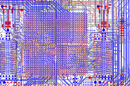
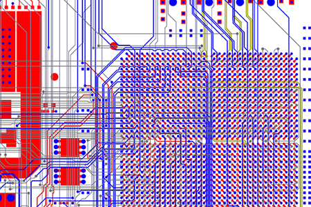
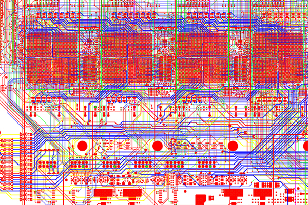 Printed Circuit Board Schematic Depicting Signal Integrity
PCB Considerations During the Circuit Design
Signal integrity challenges can often be minimized by applying proven PCB design rules early in the schematic and layout stages. Published guidelines from multiple industry sources outline best practices for routing high-speed signals, such as clocks, and explain how different design choices influence transmission line behavior.
Because many variables affect signal paths, electromagnetic interference can occur if layouts are poorly executed. Thoughtful PCB design, combined with simple and consistent design rules, helps reduce EMI and improve overall signal integrity performance.
Key design questions to address include:
- Highest operating frequency and fastest rise time in the system
- Electrical specifications at signal sources and loads
- Presence of sensitive signals requiring controlled impedance, termination, or delay matching
- Selection of microstrip versus stripline routing
- Power distribution strategy across multiple supply voltages
- Functional grouping of analog, digital, transmitter, and receiver sections
- Interconnections between independent functional blocks and their return paths
- Minimum trace widths, spacing, layer separation, and drill sizes
- Use of blind or buried vias
Traces, Vias, and Other PCB Components
Trace geometry and routing style have a direct impact on radiation, impedance, and reflections. Right-angle trace corners increase local capacitance and cause characteristic impedance changes, leading to increased radiation and reflections. Routing with two 45-degree bends, or with smooth curved traces, helps minimize these effects.
High-speed signals should be separated from low-speed signals, and digital traces should be kept away from analog circuitry. Routing adjacent layers orthogonally reduces crosstalk between layers. While vias are often necessary, they introduce additional inductance and capacitance and increase trace length. Special care is required when placing vias, and they should be avoided in differential signal paths whenever possible.
Printed Circuit Board Construction
The desired PCB stack-up depends on component packaging, signal density, and impedance control requirements. For high-speed designs, multilayer PCBs with buried ground and power planes are required. Solid copper planes allow short power and ground connections and provide low-inductance return paths for high-speed signals.
Proper stack-up selection plays a major role in maintaining controlled impedance and reducing noise. A well-planned construction supports both signal integrity and electromagnetic compatibility goals.
PCB Laminate Selection
FR-4 laminate material is widely used due to its cost-effectiveness and suitability for many digital designs, provided operating frequencies remain below approximately 2.5–3 GHz. At higher speeds, digital signals become increasingly sensitive to laminate properties.
High-speed laminates such as Rogers RO4350 offer more stable electrical properties at elevated frequencies. One key difference is dielectric constant stability across frequency ranges. Changes in dielectric constant affect signal velocity, causing different frequency components to arrive at the load at different times, which results in signal distortion. The primary tradeoff when selecting non–FR-4 materials is their significantly higher cost.
Laminate Electrical Characteristics
| Parameter | Value | Units |
|---|---|---|
| FR-4 recommended frequency limit | 2.5–3 | GHz |
| FR-4 dielectric constant (typical) | ~4.7 | — |
| FR-4 dielectric constant above 5 GHz | ~4.0 | — |
| Rogers RO4350 dielectric constant | ~3.5 | — |
| Rogers RO4350 frequency stability range | 0–15 | GHz |
Frequently Asked Questions
Quick Links
- What is signal integrity in PCB design?
- Why do signal integrity problems increase at higher speeds?
- How does PCB layout affect signal integrity?
- Why are multilayer PCBs important for high-speed designs?
- When is FR-4 no longer suitable for PCB designs?
- Can existing PCBs be redesigned or replicated?
What is signal integrity in PCB design?
Signal integrity refers to how accurately electrical signals are transmitted through PCB traces without distortion, noise, or timing errors, particularly at high speeds and frequencies.
Why do signal integrity problems increase at higher speeds?
As speeds increase, high-frequency effects such as reflections, crosstalk, and ground bounce become dominant, even on short PCB traces.
How does PCB layout affect signal integrity?
Component placement, trace routing, layer orientation, and via usage all influence impedance, radiation, and return paths, directly impacting signal quality.
Why are multilayer PCBs important for high-speed designs?
Multilayer boards with solid ground and power planes provide low-inductance return paths and support controlled impedance for high-speed signals.
When is FR-4 no longer suitable for PCB designs?
FR-4 is effective for many designs below roughly 2.5–3 GHz, but higher-speed applications may require specialized laminates with more stable dielectric properties.
How does dielectric constant impact digital signals?
If dielectric constant varies with frequency, different components of a digital signal travel at different velocities, causing distortion at the receiving end.
Need Help with Your PCBs Signal Integrity?
PCB layout is often the most significant factor affecting electromagnetic compatibility and signal integrity. Designs created solely through autorouting or rigid rule lists frequently require costly post-design fixes such as ferrites or shielding. Investing time in proper component placement and optimized routing typically results in products that meet signal integrity and EMC requirements on schedule and within budget.
Request a Quote Request Design Support Request More Information


