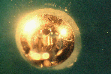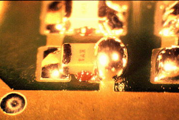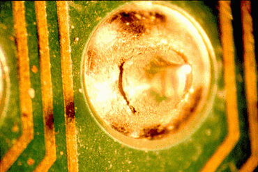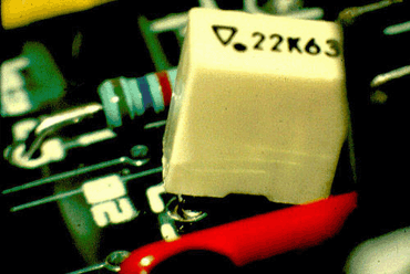
Wave Soldering Defects
Wave soldering is a large-scale soldering process by which electronic components are soldered to a printed circuit board (PCB) to form an electronic assembly. The name is derived from the use of waves of molten solder to attach metal components to the PCB. The process uses a tank to hold a quantity of molten solder; the components are inserted into or placed on the PCB and the loaded PCB is passed across a pumped wave or waterfall of solder. The solder wets the exposed metallic areas of the board (those not protected with solder mask, a protective coating that prevents the solder from bridging between connections), creating a reliable mechanical and electrical connection. The process is much faster and can create a higher quality product than manual soldering of components.
Wave soldering is used for both through-hole printed circuit assemblies, and surface mount. In the latter case, the components are glued by the placement equipment onto the printed circuit board surface before being run through the molten solder wave.
Make sure you check out our blog post titled "What Is The Minimum Pitch You Can Wave Solder a PCB?".


