Wave Soldering Defects
Sunken Joints on a Printed Circuit Board
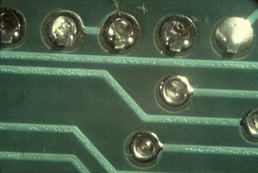
Sunken joints on the base of the board are most commonly caused by outgassing from the printed board. Like small voics in the solder fillets (referred to as pin holes or blow holes), they are seen as another process indicator. If the copper plating thickness remains a minimum of 25µm in the barrel of the hole, moisture will not outgass through the copper during soldering.
 Figure 1: Sunken solder joints caused by outgassing.
On the top side of the board, sunken or depressed joints can occur for the following reasons:
- Hole to lead ratio where the solder literally sinks due to its own weight.
- Some form of contamination or obstruction does not allow the solder to rise in the hole.
- Poor pre heat or fluxing does not allow the solder to fully wet the plated through hole.
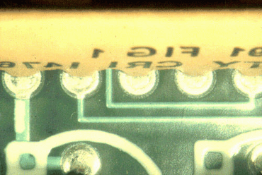
In Figure 2, the insulation on the body of the part was also found on the top of the leads, which made joint formation difficult to achieve.
 Figure 2: The component's insulation interfered with joint formation.
The most common cause of sunken joints is the hole-to-lead ratio. If the hole is large in comparison to the lead diameter, the solder literally drops in or out of the hole.
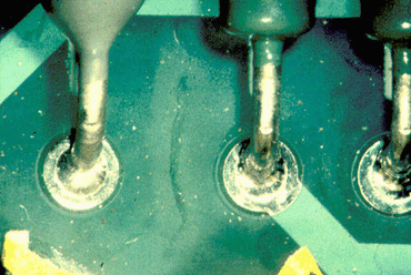
In cases where the solder has not reflowed directly on the top side of the board, sunken joints on the tops side of the board can be caused by incorrect pre-heat or poor fluxing. This would not be the case in the example shown in Figure 3 as the tin/lead has either reflowed on to the top side or caused the existing solder coating to reflow.
Sunken joints on the base of the board may be caused by outgassing. If the soldering process is functioning correctly when the hole outgasses the solder tends to shrink back into the hole to fill the void.
 Figure 3: Adhesive contamination on the pad surface caused this solder skip.


