PCB Manufacturing Process
Below are some images from the printed circuit board manufacturing process. Including, drill, plating, and final fabrication. All our circuit boards go through intensive testing and quality control during each step of the manufacturing process.
See our blog post titled Printed Circuit Board Manufacturing: Then and Now to see how the circuit board manufacturing process has evolved over the years.
Inner Layer
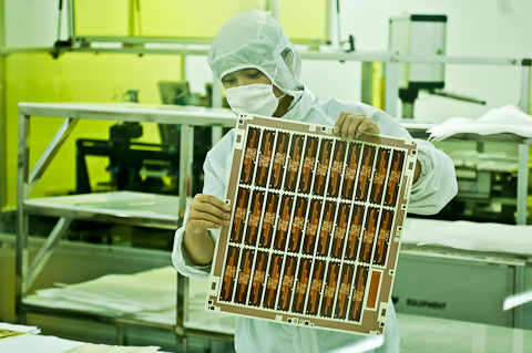
Inner layer core shown after etch\dryfilm strip processes have been completed. The core is now ready for post etch punch.
Laser Drill
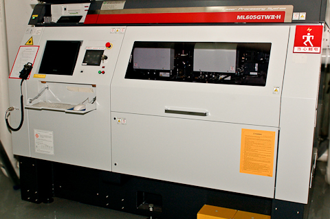
Laser drill is necessary for today growing technology, drilling the smallest micro-vias using a beam of light 20 microns (1 Mil) in diameter. High influence beams can cut thru metal and glass creating the tiny via hole.
Post Etch Punch
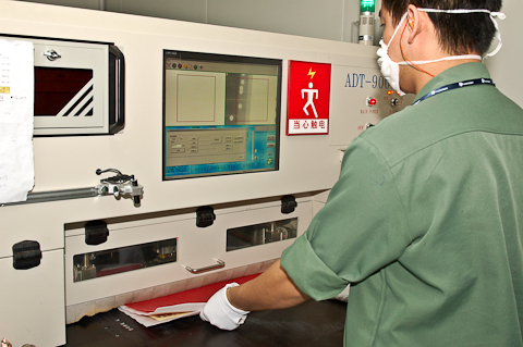
Punching core material is the only acceptable method of building precision tooling which must remain accurate in a production atmosphere.
Press Room
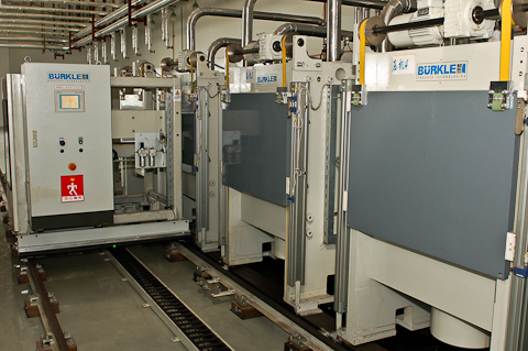
Press lines for manufacturing quality, high layer count PCBs with consistency and in a timely manner.
Drill
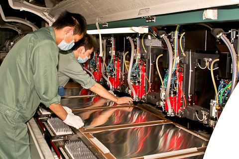
CNC machines are complete with drill and profile routing software allowing for high performance and throughput.
Plating
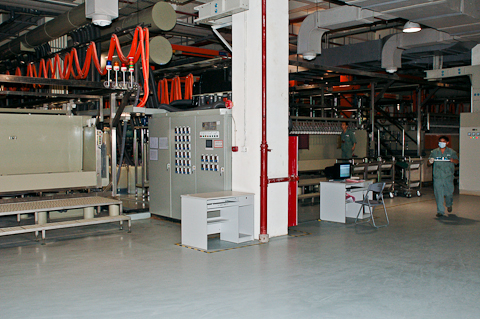
Automated plating lines serving quick turns and production of small to high volume.
Strip - Etch - Strip Line
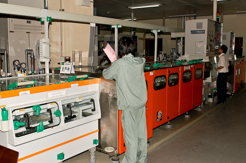
Production panels proceed to etching to remove unwanted copper and into the strip line to remove protective film.
Automated Optical Inspection (AOI)
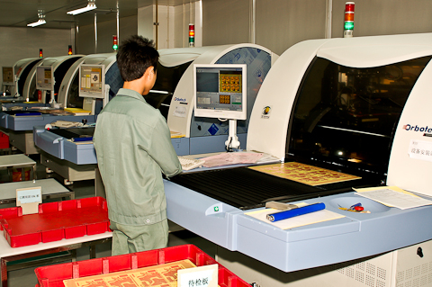
Using the latest in optical inspection equipment on internal and external layers allows for minimal fallout on final product.
Final Fabrication (Routing & Scoring)
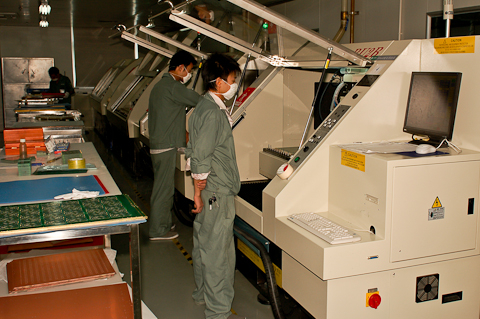
Routing and scoring to precise dimensions within supplied tolerances are the final steps prior to electrical testing. Constant monitoring by engineering ensures parts will meet your specifications.
Electrical Test
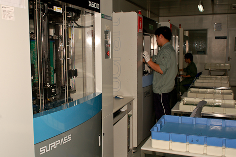
Flying Probe testers are used to 100% electrical test all PCBs on site at manufacturing.
Quality-Controlled PCB Manufacturing
Experience the difference with our rigorously tested and quality-controlled PCB manufacturing process and see how circuit board manufacturing has evolved and why our methods set us apart.
Request a Quote Request Design Support Request More Information


