Military and Aerospace PCBs: High Technical Performance for Advanced Applications
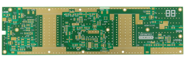
When it comes to printed circuit boards (PCBs), the military and aerospace industries have an ever-increasing demand for higher technical performance at affordable cost. Epec has made the investments in terms of both manufacturing equipment and manufacturing expertise that focuses on the high performance, reliability, and extreme environmental tolerances required for these industries. Look into it more here, IPC Class III vs. MIL Spec for Printed Circuit Boards.
Epec’s experience extends across a range of advanced laminate systems, including Isola’s Tachyon series and Panasonic’s Megtron family of materials. These high-performance substrates are engineered for low dielectric loss and exceptional signal integrity, which are essential for mission-critical aerospace and defense systems operating at high frequencies. We also specialize in hybrid PCB constructions, where materials such as FR-4, polyimide, and high-speed laminates are combined to optimize electrical and thermal performance while maintaining cost efficiency.
Additional requirements may include an expected lifetime of more than 5 years (sometimes extended to 15 years or longer). They are also required to perform in severe conditions which may include extremes of temperature, humidity, vibration, and impact, as well as survival in hostile environmental conditions such as salt spray, blowing sand or dust, and solar radiation. It is important to understand common component designs for mil-aero devices.

Military and aerospace PCBs require high technical performance to stand up to extreme environmental conditions while performing complex functions reliably. Working with a company such as Epec will ensure that the PCBs manufactured meets customer's performance specifications while being cost-effective. Some considerations that customers should know about regarding PCB requirements in these industries include wrap plating, soldermask, etchback, drilling, and hot air solder leveling (HASL) processes.
Security and Compliance: Trusted ITAR Manufacturing for Defense and Aerospace
The military and aerospace sectors demand more from printed circuit boards: greater technical performance, long-term reliability, and absolute trust in the security of sensitive data. Epec delivers on all fronts by combining advanced manufacturing capabilities with rigorous quality and cybersecurity standards.
In addition to our high-reliability engineering and production processes, Epec is a fully ITAR-registered manufacturer, authorized to handle and produce defense-related technical data and products in accordance with the U.S. Department of State’s International Traffic in Arms Regulations (ITAR). This registration enables us to build PCBs and other electronic components that are critical to national defense and subject to export control. We strictly control all access to ITAR data, enforce security measures for data transmission, and require verification for any personnel or subcontractors accessing controlled information.
Our ITAR-controlled PCB manufacturing includes rigid, flex, and rigid-flex circuit boards, from standard 2- and 4-layer builds to advanced designs featuring blind/buried vias, HDI, and 3 mil lines/spaces. We've made significant capital investments in automated precision equipment, laser drilling, plasma etching, optical registration, and CNC routing to ensure consistency, high yield, and full compliance with AS9100 and MIL-spec requirements.
Within our ITAR-controlled manufacturing environment, we regularly build boards using Tachyon and Megtron laminates for defense radar, avionics, and satellite applications that demand ultra-low signal loss. Our controlled processes for hybrid multilayer stack-ups ensure precise dielectric consistency across layers, even when combining different resin systems or copper weights.
Security goes beyond physical product control. Epec has built an information infrastructure designed to meet the strict requirements of NIST SP 800-171 and the evolving Cybersecurity Maturity Model Certification (CMMC) framework. These standards mandate strict controls over Controlled Unclassified Information (CUI), including access restrictions, system security plans, encryption protocols, and continuous monitoring. Our IT systems, internal protocols, and third-party partnerships are structured to ensure compliance and eliminate risk to our defense and aerospace customers.
Whether you need prototype support or full-scale production, Epec combines manufacturing excellence with unmatched data and security discipline, making us a trusted partner for secure, high-reliability PCB manufacturing in defense, aerospace, and other ITAR-regulated industries.
What is Wrap Plating?
Wrap plating is where the drill hole is plated with copper as the plating extends from the hole drilled onto the board and onto the surface. This plating is made from copper; it extends from around the via structure and under the cap plating to move out from the surface. Learn more about PCB Wrap Plating: the critical process in circuit board manufacturing.
There are different class specifications regarding the thickness of the electrolytic hole plating thickness. The IPC-6012 standard (and IPC-A-600 inspection standard) has a Class I, Class II, and Class III categories. Class I thickness specifications merely state that the thickness will be as agreed between the user and the supplier (AABUS). This is the least option used by most production facilities.
The Class II specification is where the wrap plating has to be continuous through the filled plated hole and it becomes extended on the PCBs surface. The thickness of the wrap plating can be no less than 5 μm [197 μin] for the via structures and through-holes. Also, the processing of the circuit board by means of planarization, sanding, and etching processes should not result in having insufficient wrap plating in place when these processes reduce the thickness of the copper material.
The Class III standard is similar to the Class II standard except that the minimum thickness of the wrap plating should not be below 12 μm [472 μin] for the through-holes, blind vias, and buried vias that are greater than 2 layers. Buried via cores must have a minimum thickness of 7 μm [276 μin] and both blind and buried microvias can have a minimum wrap thickness of 6 μm [236 μin].
There are many challenges associated with wrap plating of the PCB. Knee cracking is when expansion of the plating during thermal cycles of the PCB can result in the wrap plating developing stress cracks due to the temperature, number of PCB layers, and the CTE of the materials. Butt joint failures can also be a result caused by thermal cycles. Another challenge is meeting the minimum thickness standards during the planarization process that could vary the thickness of the wrap by ±0.3 mils.
When manufacturing hybrid and high-speed designs with advanced materials like Tachyon and Megtron, maintaining consistent wrap plating thickness is especially critical due to differing coefficients of thermal expansion (CTE) between materials. Our process controls and automated inspection systems allow us to manage these variations effectively, preventing stress cracking and maintaining Class III reliability.
What is Positive Etchback and Negative Etchback?
PCB etchback is a process that removes the epoxy resin that formed along the sidewalls of the via that was caused when the PCB hole was drilled. The drilling process can cause the temperatures to rise greater than the substrate's glass transition temperature and melt in the plated through hole (PTH). By removing the epoxy, it ensures good electrical connectivity for the PCB layers. There are two types of etchback processes: positive etchback and negative etchback. Check out this blog post, PCB Through Hole Plating: PCB Etchback vs Standard PCB Vias and Holes.
Positive Etchback: This cleaning process involves having the dielectric material cleaned back within the hole walls so that the copper land will protrude past the edges of the PTH. This process is commonly used for military, medical, and aerospace industries so that a strong three-terminal contact can be made to ensure superior reliability and performance.
For high-speed and RF applications using Isola Tachyon or Panasonic Megtron materials, we apply tailored etchback profiles that account for resin hardness and glass weave structure. These controlled processes help preserve interlaminar adhesion and ensure copper-to-copper integrity across hybrid dielectric systems.
One processing challenge to be aware of is when using laminated PCB boards such as the Rogers 4000 series. Due to how the PCB's materials for the laminated board are made, etchback is typically not recommended as the process can loosen the hole wall's filler particles when removing the resin near the copper layers.
Negative Etchback: For the negative etchback process, or commonly known as desmear, the epoxy resin is cleaned from the plate holes as the copper land becomes recessed from the edges of the hole walls. This process is not typically recommended for PCBs used in the military or aerospace industries.
What Occurs During the PCB Drilling Process?
The drilling on the PCB is one of the most complicated and time-consuming processes. Even the slightest error is irreversible and will result in the loss of the PCB. The drilling can be done using either mechanical means or with laser drilling to create the desired hole diameter. There are two types of drill holes that are made: plated through holes (PTH) and non-plated through holes (NPTH). PTH are conductive vias or component holes that will carry the signal as there are interconnections between the PCB layers. NPTH are non-conducive used as mounting or standoff holes, or for holding components in place during the PCB assembly process. Here is important information regarding aspect ratios and drill sizing, PCB Mechanical Drilling vs. Laser.
Watch Our Video
Lenz DLG-550 in Action: High-Speed, High-Accuracy PCB Drilling
What are the Current Soldermask Applications?
Soldermask is a polymer layer that is placed onto the PCB to protect all the metal elements from the effects of oxidation. This process also helps to prevent conductive bridges from forming from one solder pad to another. There are several different types of soldermask such as liquid epoxy thermosetting, liquid photoimageable solder, and a dry film solder mask. In most PCB facilities, dry film application has been replaced with liquid. More on this topic here, Circuit Board Solder Mask - What to Use and What Not to Use.
Once the soldermask is applied, the PCB will be cured and finished. The liquid epoxy soldermask goes through a thermal curing process, while both the liquid photoimageable and dry film solder undergoes an ultraviolet (UV) exposure that is done within the photolithography process.
Soldermask can come in a variety of colors as the dyes are from within the soldermask materials. The dye colors are important during the inspection phases of the PCB, as the dyes allow the traces to be seen during both manual and automated inspections. The green soldermask is the most common dye color and can assist both inspection types, while other colors such as black can make automated inspections difficult. It should also be noted that the chemicals in the dyes can sometimes vary the thickness of the soldermask dams. Significantly opaque masks require specialty processing and can be more difficult to adhere.
Soldermask used for military and industries that require high reliability will fall under the IPC-SM-840C Qualification and Performance of Permanent Solder Mask specifications that helps designers, manufacturers and users monitor the acceptability of the soldermask offered by the vendor.
What is HASL and How Does It Compare to Tin Lead Reflow?
Hot air solder leveling (HASL) is a PCB finishing process where the PCB is dipped into molten solder consisting of approximately 37% lead and 63% tin after the soldermask has been applied. Next, a hot air solder leveling machine uses hot air (air knives) to remove any excess solder from the PCB as only a very thin layer is left. This finish is one of the most common processes used today.
The main benefit is to protect the traces that are underneath the PCB from corrosion. The HASL also helps to pre-tin the circuit board's pads so components are easier to solder onto it during the PCB assembly phase. Main disadvantages include creating an uneven surface from the finish, having the solder plug, reducing the plated through holes (PTH), and solder bridging. Find out the advantages and disadvantages of printed circuit board surface finishes.
Tin lead reflow process may also be used to finish PCBs. This process involves where the PCB, mounted components, and tin lead solder paste is pre-heated as the board reaches a temperature near the melting point for the tin lead solder paste. The tin lead solder then turns from a solid to a liquid as it flows across the PCB to cover the areas that are not protected by the solder mask. Then the PCB is cooled down.
One of the biggest differences between HASL and tin lead reflow is that HASL process uses a molten solder dipping procedure to entirely coat the PCB, while tin lead reflow uses a solder paste that is heated along with the PCB. Also, when it comes to tin lead reflow, temperature control is paramount.
If the temperature is increased too quickly, the tin lead solder could bubble and splatter as solder balls would get onto the components. If the temperature is increased too slowly, the tin lead will oxidize while forming solder balls. Also, if the temperature changes too rapidly, it could cause damage to components from heat stress. If you're interested, take a look at why lead free HASL finish is a hassle.
Watch Our Video
Hot Air Solder Leveling (HASL) Explained: How It Protects PCB Finishes
Military Flex and Rigid-Flex PCBs
The next level of flex and rigid-flex PCBs is being able to design and manufacture parts in the U.S. for ITAR, military, and aerospace applications. Learn more about these highly complex and high-reliability applications.
PCB Prototype and PCB Production
Epec has a proven track record with PCB prototype and PCB production using standard and advanced technologies for the aerospace and military markets. You can view some of the specifics around our production capabilities and specifications below for standard rigid PCBs, flex/rigid-flex PCBs, and heavy copper PCBs that we have developed and perfected in conjunction with many of the largest military and aerospace companies in the world.
Along with our standard PCB capabilities, the list below is in addition to that substantial set of capabilities.
Certifications:
- MIL-PRF-55110
- MIL-PRF-50884
- MIL-PRF-31032
- IPC Class III
- AS9102
- ITAR Registered
Materials:
- FR-4
- Polyimide
- Arlon
- Flex & Rigid-Flex
- Hybrid Constructions
- Embedded and Printed Resistors
Our material expertise includes extensive experience building multilayer PCBs with Isola Tachyon, Tachyon 100G, Panasonic Megtron 6, and other high-speed dielectric systems. These laminates are commonly used for radar, RF, and satellite communication hardware. In many cases, we design and produce hybrid PCB stack-ups, blending high-speed materials with polyimide or FR-4 cores to achieve an optimal balance between performance and manufacturability.
Copper Weight:
- UL up to 6 Ounces
- Heavy Copper Capabilities
- Multiple selectively plated copper weights on external layers
Specific Process Capabilities:
- Sequential Lamination
- Blind & Buried Vias
- Filled Vias (Conductive and Non-Conductive)
- Laser Drilling and Stacked Vias
- Metal Clad & Heatsinks
- Edge Plating and Castellation
- Air Pockets/Cavities
- Microwave & RF PCBs
- Controlled Impedance +/- 5%
- Plated Countersinks/Slots
- Controlled Z-Axis Routing
Manufacturing for Critical Applications
Epec has over 70 years of experience in building circuit boards for these critical applications. We’ve sent PCBs on the Apollo 11 mission and we take pride that all circuit boards manufactured for military and aerospace applications require fixed and approved origins of manufacture with total traceability and security of Gerber data and engineering specifications. All our systems for quality and security have passed audits from the DOD, FDA, FAA, and most of the Tier 1 defense contractors.
Not only do we provide manufacturing expertise, but we also typically work very closely with our customers’ engineering teams on their designs. Because we understand that these products must operate in harsh environments, we utilize materials capable of withstanding extremes of stress, pressure, and temperature as part of our services.
Our experience with Tachyon, Megtron, and other advanced dielectric systems allows us to deliver consistent electrical performance across wide temperature ranges and high signal frequencies. In hybrid builds, we ensure precise layer registration and impedance control, critical for RF, radar, and communication circuits where every mil of deviation matters.
Experience Unmatched Reliability
Whether your design calls for Tachyon 100G for low-loss performance, Megtron 6 for advanced high-frequency applications, or a custom hybrid construction, Epec’s engineering and manufacturing teams have proven experience to deliver boards that meet strict aerospace and defense specifications.
With over 70 years in the PCB industry, with certifications to back it up, and a track record of excellence, we offer performance you can trust. Ready to make your project soar? Contact us now for a custom quote.
Request a Quote Request Design Support Request More Information


