Plated Shut Through Hole Vias
Many veteran PCB designers have experience with the use of plated shut microvias, which many but not all PCB fabricators can provide. Over the past several years, our NetVia Group facility in Dallas has developed a process that allows us to plate shut through hole vias, up to 12 mils in diameter, without concern of voids, air pockets, or fluid entrapment in the holes.
Traditionally, when a PCB designer needed a through hole filled, they would specify a conductive or non-conductive via fill, which is becoming a standard process that most printed circuit board fabricators have invested in.
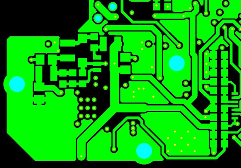 Through vias are illustrated in blue and copper plated shut vias are shown in yellow.
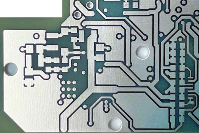 Actual circuit board with copper plated shut vias
However, for the most technical applications, copper plated shut vias have several advantages:
- No depression on the cap plate: With the via fill process, there is always going to be a slight depression on at least one side of the hole (sometimes both depending upon how it is processed) based upon which side of the panel the material entered the hole as well as the contraction of the fill during the cure cycle. With plated shut vias, a depression is eliminated being that the entire hole is filled with copper and slightly protrudes the surface prior to planarization.
- 10X improvement in thermal conductivity: Non-conductive fill has a thermal conductivity of 0.25 W/mK, whereas conductive pastes have a thermal conductivity anywhere from 3.5-15 W/mK. In contrast, electroplated copper has a thermal conductivity of more than 250W/mK, so for the most demanding applications where thermal management is key, there is no better solution.
- Improved signal frequencies: It is common knowledge that conductive losses along a transmission line in a PCB will increase due to heating at the surface of a trace and due to leakage between the transmission line and its reference conductor. Through holes filled with conductive materials are not as effective for the transmission of high-frequency signals due to creating resistances at high frequencies versus copper filled through holes.
Process Methods
Plated shut through hole vias cannot be done using traditional PCB plating methods as these processes will create quality defects that will not be seen until the PCB is under thermal stress. Our process has been proven to ensure that you will not have any voids or outgassing in your through holes, as you can see from these cross-section photos showing complete copper fill.
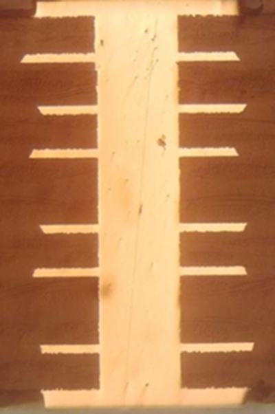 Cross Section of 12 Mil Hole on 62 Mil Thick Multilayer PCB
The only tradeoff to this technology is that it takes longer to process and costs more than the traditional filled via process, but the thermal advantages are so significant that in many applications there is no comparable substitute to the quality and performance.
The plated copper filling process also makes for a solid core so, you will get a flat surface to be plated, and this prevents the solder from dispersing and affecting the solder joint at the assembly level.
In the past, this process has had some limitations as traditional plating process make it very difficult to plate the whole barrel smoothly without air or liquid being trapped in the middle. Standard plating chemistries and process tend to deposit copper in high throw areas at a greater rate than low throw areas (via barrel), the possibility of plugging the surface of the via prior to the center is extremely high. In this event, plating chemistries will be trapped in the via, creating a void.
The use of a single copper plating solution in a single step using DC chemistry is typically viewed as the "ideal" process for filling through holes with copper as it minimizes the number of plating tanks and shortens the overall dimensions of the physical plating line. Plating times of greater than 15-18 hours can be required to fill a through hole in a thick substrate utilizing DC plating chemistries.
Need Help with Plated Shut Through Hole Vias?
Unlock superior thermal performance and signal integrity with our copper plated shut vias. Experience the difference today.
Request a Quote Request Design Support Request More Information


