Differences Between Through Hole and Surface Mount PCB Designs By Al Wright, PCB Field Applications Engineer Epec Engineered Technologies
One of the first decisions involved in laying out a printed circuit board (PCB) is choosing the type and style of components to be used. This decision is mainly driven by the PCB’s electrical requirements, but once those are satisfied, it is often possible to choose from a variety of available configurations and footprints for common component types, such as resistors, capacitors, and diodes. The component types selected will influence the size and appearance of the finished printed circuit board assembly (PCBA).
In the past, components with long leads would be inserted, usually by hand, into plated through holes on the PCB. The leads would then be soldered to form permanent interconnections with the holes. This was known as through-hole assembly.
Increasingly though, designers prefer to use a more modern (though by now fully mature) assembly method which utilizes components whose leads attach to the PCB surface only, without the need for a mating hole. This method, originally known as “planar mounting” has since become more widely known as surface mount technology (SMT). Get the full story on Plated Vs Non-Plated PCB Through Holes in PCB Designs.
The following is a concise comparison between the through-hole and SMT methods for use as a decision-making reference guide for PCB designers.
Through Hole Technology
While through-hole components represent the older of the two technologies, there are still valid reasons for using them. For example, any hobbyist with a soldering iron can assemble a through-hole PCB or a small lot of the same with a minimum of fuss because the holes which accept the component leads are spaced farther apart than the surface pads on an SMT type. Typical spacing from hole center to hole center is generally 0.100” or greater, even for DIP processors. Such generous spacing makes through-hole PCBs easy to hand-solder. There is almost no potential for accidentally creating bridges between the pins on a single component or between those on adjacent components. This cuts down on troubleshooting and rework once the board is fully assembled and powered-up.
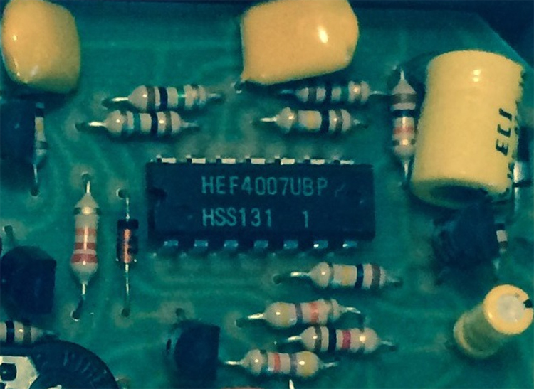 Through-hole PCB with 14-Pin DIP. Lead spacing for DIP is 0.100” x 0.300”, with 14 holes and associated pads.
Through-hole boards can also be useful in more professional settings, particularly at the prototype stages of a project. The prototype layout can temporarily use through-hole components so that the board may be assembled quickly for basic proof-of-concept evaluation. After the board has been proven to function correctly, the designer can swap-in smaller SMT types of the same values and revise the PCB layout within a smaller footprint for final testing and eventual production. Doing things this way may save up-front costs for a project, especially those associated with subcontracting a small lot to an outside assembler. Keep in mind that small lots often command premium pricing from outside service providers, who naturally prefer to set up large volume production runs that keep their machines going.
Cost Saving of Through Hole Technology
One cost saving for a through-hole PCB is that there is no need to generate a new solder stencil each time the PCB undergoes a revision change. This can save hundreds of dollars on a design which goes through two or three spins before it is deemed to be functional. It is also unnecessary to set up pick-and-place equipment, or to purchase accompanying reels of SMT components, until the final PCB configuration is working and ready for production.
In-circuit testing after component assembly can often be done manually and in-house for a small batch of boards, thereby eliminating the expense of fixtures or associated setup charges. The final advantage is that it is possible to use tin-lead solder (the least costly surface metalization) when working with through-hole boards. The inherent non-planarity of HASL, which can make placement of fine-pitch surface mounted components difficult, is not an issue on through-hole designs.
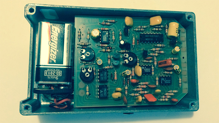 A through-hole PCB in a hobbyist application, in this case a guitar effect pedal. Notice the ICs, which are all either 8-pin or 14-pin on 0.100” x 0.300” centers.
Another advantage beyond the avoidance of SMT-related cost adders is that it is possible to evaluate mechanical issues (such as excessive warp and twist) during validation, and to compensate for them during redesign, without causing insurmountable assembly difficulties, as might occur with SMT. This is because warp and twist is not nearly as critical on a hand-assembled PCB as it is on one populated using pick-and-place equipment. A human assembler can simply change their wrist angle to improve the fit of a stubborn component, but an automated machine requires a PCB with a high degree of flatness in order to function properly. Your through-hole prototype can expose design-related mechanical shortcomings before they become costly and time-consuming “line-down” three-way screaming matches between your PCB fabricator, your contract assembler, and yourself.
In summary, when the necessary component types are available in through-hole form, the use of through-hole technology during the development cycle can keep your project on track and can simplify the process of assembling prototype and small-lot projects without paying for third party services. Timelines may be more predictable and controllable with fewer side issues that might delay your product’s critical time-to-market. It may therefore be worth considering at least the temporary use of through-hole components during early development and validation stages, whether you as the end user are a hobbyist, an industry start-up, or an established electronics supplier.
Surface Mount Technology
Regardless of the justifications above for using through-hole components on your PCB, surface mounted components offer many advantages that through-hole types simply cannot match.
One of the most immediately obvious advantages is that it is possible to achieve far greater levels of component density and processing power while fitting everything within a much smaller and lighter overall PCBA. As the devices controlled by PCBs become smaller and smaller, efficient use of available surface area becomes increasingly more critical. SMT technology becomes a necessity.
For instance, it would require several 14-pin or 16-pin dual inline processors, each measuring around 0.80” X 0.35”, to even approximate the computing power available in a single surface-mounted BGA or 64-pin QFP processor which might fit within a total area one square inch or smaller. In addition to the larger component footprints for through-hole types, the interconnections on the PCB would require additional space for via placement.
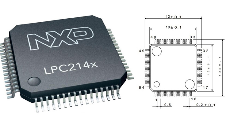 Miniaturization on the march: The 64-pin surface-mounted QFP processor measures only 0.472” x 0.472”.
By contrast, when using SMT components, the plated through-hole required for each through-hole component lead is eliminated and is replaced by a relatively small surface pad. It is then possible to drill small vias into the surface mount pads themselves, directly underneath the SMT component leads, allowing for Z-axis interconnections which can then fan out from the wall of the via to one or more internal signal layers. All of these interconnections can now occur either within or immediately adjacent to the device’s own footprint, saving very significantly on available real estate. The space around the SMT component can then be used for placement of additional components. The higher densities possible with SMT are a byproduct of both the smaller footprint size of the components themselves and the space reclaimed by the elimination of drilling component mounting holes. A related advantage is that it is common for SMT boards to utilize both sides of the PCB for component mounting.
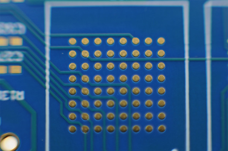 64-pin SMT BGA, 0.031” pitch. Notice that the ball pads have small dimples, indicating that they have been used for placing vias-in-pads to allow for internal layer escape routing.
With such advantages come several considerations which must be kept in mind when designing for SMT PCBs. Materials, surface finishes, and mechanical characteristics become increasingly important. Problems with any of these elements can cause major headaches when it comes time to assemble the PCBs on automated equipment.
Surface Mount Design Considerations
Materials and surface finish play a critical role and are to some extent interactive with one another. The leaded solder used in HASL is a poor choice for SMT work (particularly on components with pin pitches less than 0.050”) because it tends to puddle at one end of the pad, where it then cools in a non-planar state. The component leads need to sit flat in order to avoid positioning problems, so even when RoHS compliance is not an issue, it is best to select a more planar finish such as ENIG, Immersion Silver, or Immersion Tin when dealing with finer-pitch SMDs.
It is also very important not to under-spec your base laminate. SMT boards generally require higher soldering temperatures than through-hole boards, primarily because of the lead-free surface finishes that are most often used. Materials that meet IPC-4101D/126 (Tg 170C, Td 340C, with inorganic fillers) will stand up to high soldering temperatures. They will also withstand multiple thermal cycling shocks which will occur when assembling two-sided SMT boards, or boards which use multiple component technologies.
Gerber artworks need a few extra features so that the SMT assembly process will go smoothly. Add at least one set of fiducial pads to the external layers (most commonly in an “L” pattern along the outer edges of the PCB) so that pick-and-place equipment will have a reference for squaring the PCB and for establishing a dimensional datum point. Consider eliminating soldermask openings for vias to minimize the potential for solder shorts and to eliminate reflections that may confuse the pick-and-place unit when it is trying to identify the fiducials.
For in-circuit testing, it is often good practice to add test point pads wherever you need them. Depending upon the test equipment, these can be SMT type or they may include holes to accept test probes. Work with your assembler or test service to determine which type is best.
Given the importance of dimensional accuracy and the nature of automated assembly equipment, it is very important to “design-in” flatness. Do this by balancing copper coverage as evenly as possible from layer to layer and by pouring copper into large blank areas wherever you can. This will prevent uneven stresses from pulling the material in a particular direction after etching.
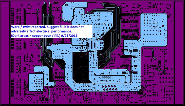 Internal layer for a SMT PCB. The dark areas were originally devoid of copper on several internal layers, which allowed the PCB to twist under thermal stress. Our suggestion was to pour additional copper into the blank areas to even out the layer-to-layer stress.
Use stack-ups which are symmetrical around the center of the stack so that the layers support one another in the Z axis. For example, a six-layer PCB will generally stack as follows: Top Signal L1, Prepreg, Plane L2, FR4 core, Internal Signal L3, Prepreg, Internal Signal L4, FR4 Core, Plane L5, Prepreg, Bottom Signal L6. This will work as long as the copper area on each layer is fairly well balanced (particularly on the core layer pairs at L2-L3 and L4-L5) and it will place planes where they will be available as reference for impedance control at layers 1+3, 4+6.
If you build a prototype and it does warp or twist, do not attempt to “fix” the problem by adding a drawing requirement for warp and twist that is in excess of what IPC requires. The IPC warp and twist spec are already twice as stringent for SMT as it is for through-hole, and most fabricators will push back if you ask for anything tighter. Instead, revisit the design for potential causes of the problem, and be sure that you understand when the problem is happening – on the bare PCBs as-received, during assembly, or both. Then work with the fabricator, who can often make recommendations that will alleviate the problem on subsequent runs.
Summary: Through-Hole or SMT?
The information above is intended to explain the main differences between through-hole and SMT technology for consideration when planning a new PCB design project. While SMT is by far the more common technology over the past several years, through-hole can still fill certain needs, so long as it can deliver the necessary processing power within a reasonable footprint size. It is useful to consider both PCB types and to weigh their pros and cons before launching your development cycle.
Table 1: Comparison of Characteristics
| Through-Hole | Surface Mount |
|---|---|
| Non-planar HASL finish most common. | Planar finish (ENIG, Immersion Silver, OSP.) |
| Hole required for component lead insertion. | Components mount to surface pads, no hole. |
| 2-sided assembly rare. | 2-sided assembly common. |
| Component lead spacing typically 0.100” or greater. | Component lead spacing 0.0157” (0.0197” common.) |
| Manual assembly. | Automated assembly. |
| Soldering manual or automated. | Soldering typically automated. |
| Stencil not required. | Stencil required unless small lot, simple PCB. |
| Vias in pads not possible. | Vias in pads possible. |
| Standard temperature (130C Tg) laminate. | High-temperature (170C Tg) laminate. |
| Through-hole test points. | Through-hole or SMT test points. |
| Lower component and circuit density. | Greatly increased component density. |
| Larger PCB footprint. | Minimal PCB footprint. |
| Rework relatively simple. | Some rework more involved. |
| Moderate warp and twist tolerable. | Warp and twist more critical for assembly. |
| Fiducial pads not required for component placement. | Fiducial pads required for automated pick-and-place equipment. |
Looking For Engineering Support For Your PCB Design?
Our team of experienced engineers is here to help you with all your circuit board needs from design, prototypes, and production.
Request a Quote Request Design Support


