EXTREME Copper PCB Capabilities Webinar
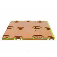
An increasing number of power electronics products are taking advantage of a growing trend in the printed circuit board industry: Heavy Copper and EXTREME Copper Printed Circuit Boards.
Most commercially available PCBs are manufactured for low-voltage or low power applications, with copper traces or planes made up of copper weights ranging from 0.5 oz/ft2 to 3 oz/ft2. Heavy copper PCBs can have more than five times that copper weight, and EXTREME copper PCBs can range up to 200 oz/ft2.
In this webinar we will discuss design considerations unique to this product as well as how much current these boards can carry. The minimum conductor width and spacing and cost trade-offs for the different techniques will also be covered.

Watch the Recording Below
View the Presentation Slides
View the Slide Deck on SlideShareWebinar Agenda:
- Increased endurance to thermal strains.
- Increased current carrying capacity.
- Increased mechanical strength at connector sites and in PTH holes.
- Use of exotic materials to their full potential (i.e., high temperature) without circuit failure.
- Reduced product size by incorporating multiple copper weights on the same layer of circuitry.
- Heavy copper plated vias carry higher current through the board and help to transfer heat to an external heatsink.
- On-board heatsinks directly plated onto the board surface using up to 120-oz copper planes.
- On-board high-power-density planar transformers.


