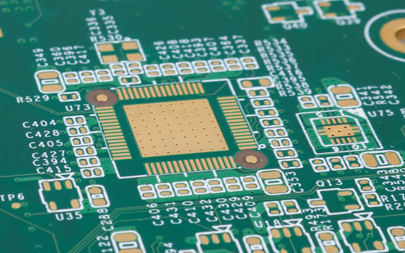
Why High-Tech Multi-Layer PCB Features Add Cost and Processing Time
There are many special features that are designed into the printed circuit board (PCB) that will increase the number of processing steps that it takes to complete the order. The combination of features can add additional cost to the raw PCB and increase the lead time to process.
When considering a PCB design and layout or redesign, it would be advantageous to consult with experts. Your printed circuit board supplier should have engineering resources to consult and review preliminary information and be able to assist with design suggestions.

In this webinar we discuss multilayer features for printed circuit boards that add cost and processing time. We will also look at base costing materials, copper weights, common cost adders, plating finishes, processing, less common features, and more.
Watch the Recording Below
View the Presentation Slides
View the Slide Deck on SlideShareCheck Out the Full Q&A
We have compiled all the questions submitted at the conclusion of this webinar into a readable format available on our blog.
Webinar Agenda:
- Base costing: Materials, X, Y, copper weight, final thickness, surface treatment, layer count
- Common cost adders: Copper >2oz, impedance, higher temperature material, RoHS finish
- Not as common features: Blind/buried vias, stacked vias, via-in-pad, plated slots
- Less common features: Cavities, plated edges, milling, castellated holes, counter bore/sink, back drilling
- Plating finishes: HASL – phasing out still, RoHS – ENIG, ENEPIG, immersion silver, LF-Hasl, immersion tin, OSP, combined with selective hard gold, gold tabs, carbon ink, selective ENEPIG
- Processing: Drilling, lamination, plating, soldermask, routing, scoring, electrical test


