PowerLink PCB with Multiple Copper Weights Helps Power Aerial Drone
Challenge
Epec was approached by a company that specializes in the development of aerial film drones to implement heavy copper printed circuit boards (PCB) in their current design. The customer’s existing line of small to medium sized drone aircraft are used for remote TV and film production, as well as for thermal imaging. The customer was looking to incorporate a heavy copper PCB feature into their newest design that would allow for a transfer of 500VDC@150A through a compact PCB.
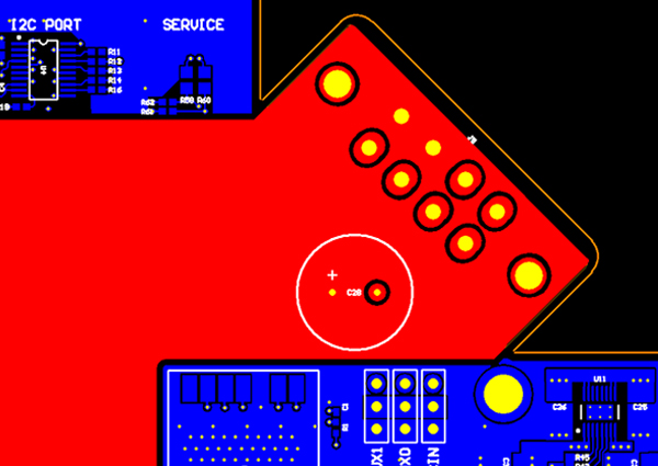
In addition to the heavy copper for power distribution, the PCB layers needed to have areas of light copper for placement of surface mounted components. Otherwise, the pitch of the components would have been too fine to etch accurately on 10oz copper. Heavy copper on the entire layer would also have imposed a weight penalty, resulting in decreased battery life and flight time. A decision with Epec and the customers engineering team led to selectively plating only the power distribution areas to 10oz of copper.
After the initial phone conference to discuss design options and limitations, we received a concept drawing and a basic outline. The concept drawing showed the approximate configuration of the completed assembly, along with the approximate area available for heavy copper plating. The basic outline showed the demarcation lines for the two different copper weights. Epec’s PCB Field Applications Engineer, Al Wright, marked up the drawing with notes taken during the phone conference so that all of the requirements would be present on a single document for accurate quoting.
Solution
A preliminary PCB quote was supplied with two included options. One option used only 1oz copper, the other used 1 and 10oz copper. The purpose was to find out how much the selective heavy copper plating added to the price of these circuit boards, and how the overall price compared to their previous method of connecting the power section. The customer liked the pricing and their engineering team preceded with the layout the printed circuit board.

A list of design rules for the 10oz areas of the printed circuit board was supplied to the customer’s layout engineer. The first set of PCB data files submitted were very good and were close to what was needed to successfully manufacture these boards. There was however one very dangerous defect. There was an area where the customer’s Gerber files used a self-intersecting polygon. This would cause the copper fill to collapse inside of the “keep-out area” and flood into the component area. This small design flaw would have caused fatal shorting had it not showed up in a warning during importation for the design for manufacturability (DFM) check. After the problem was reported, their PCB designer was able to change some export settings to correct it. The second set of data files were good and ended up being the set that we ultimately used for production.
Result
Production of the initial lot of heavy copper circuit boards went very smoothly. In this case, the customer had come in with a pretty good idea about how they could apply the PowerLink technology to a product similar to others that they were already building.
By engaging with our engineering team at the beginning of the project and by following our recommendations for manufacturability, the customer was able to create good data files very quickly, and the files became the basis for a successful prototype run.
During the past week (about 6 months since the beginning of the first project) we received a set of manufacturing data files for a similar design. The biggest difference is that the new design uses 4-layers instead of 6-layers. This time, the files were in even better condition, needing almost no modification to make them 100% production-ready. We look forward to another successful build for manufacturing heavy copper PCB’s used in aerial drones.
Need Help With A Heavy Copper PCB Design?
From design to production, our team of experienced engineers at Epec is here to help you design a production ready circuit board for your application.
Request a Quote Request Design Support


