Utilizing Shielding Films to Improve Flexible PCB Bend Requirements
Challenge
This customer, a reputable OEM for instrumentation equipment, came to us by submitting a quote request through our website. They downloaded our flex and rigid-flex circuits design guide and received some information, however, their design was more involved than the scope of the material on our website. They then reached out to us for additional support through our inside sales team.
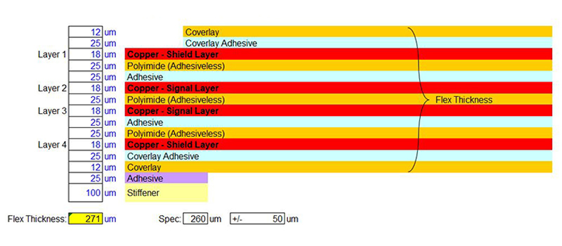
They had a flex circuit design that required shielding on both sides to meet their EMI and RF requirements. They were not sure as to what the optimum solution would be. They were looking at it from the perspective of a rigid circuit board, where in that scenario you would typically just add additional copper layers to the external sides of the part. Applying this method to a flexible circuit board design, you are increasing the flex thickness, restricting the flexibility, and potentially not meeting the bend requirements.
 Original 4-layer flex PCB copper shield stack-up.
For flex circuits, other options can be considered beyond adding additional copper layers. The preferred solution is to utilize specialized shielding films that were specifically developed for the flex PCB industry. For these types of applications, we rely on Tatsuta out of Japan, as their materials are probably the best in the industry.
Solution
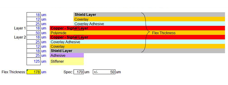
After we reviewed the customer’s design requirements, we determined that it was a very good candidate for the use of shielding films on the external layers as opposed to copper layers. This solution would minimize the flex thickness, allowing their bending capabilities to be met, and as an added benefit, reduce the part cost.
As an organization, our business model for our flex circuit product line, as well as others, is focused on design support with our customers. In this case, the customer was extremely pleased with how quickly we responded and the information we provided. When Epec is engaged early in the design phase, we can provide better solutions for our customers.
In this case, the solution was derived from their original concept, which was a 4-layer flex PCB construction. Our engineering team and product manager had a conference call with the customer discussing the usage of shielding films and we were able to show them a different solution than what they originally were thinking.
We were then able to take their original design and create a preliminary construction and data mockup, converting it to the use of the shielding films, that the customer was then able to review. They developed an understanding of what we were proposing and were able to update their data set accordingly, while we were still required to provide some additional design support. The reason being is that shielding films are not handled well in most CAD systems; the CAD systems don’t understand them. The customer did the initial configuration of the shielding films as they understood it, and we incorporated some additional adjustments, to the shield layers, for spacing, open features, and the extent of the coverage, etc.
 Revised 2-layer flex PCB Tatsuta shield stack-up.
An additional element is that shielding films connect to the flex design uniquely. They're not connected through plated holes or vias as you would see in a rigid circuit board. Shielding films connect through selective multiple openings in the coverlay layers that expose the ground circuit in the underlying circuitry. The shielding films have an electrically conductive adhesive. When laminated onto the surface of the coverlay, the adhesive extends down into these openings and bonds both mechanically and electrically to the ground circuit in the design. This is a method that CAD packages are typically not configured to apply. It is very common for us to modify the shielding layers to account for both manufacturing tolerances and to add the appropriate coverlay openings for the shields to interconnect to the ground circuit.
Result
Once we had informed the customer of the available shielding options, we worked with them to evolve their design to utilize the shield layers, and we progressed through to a finalized production-ready dataset.
The savings they received fell into two categories. First and foremost, it was a design improvement, ultimately helping to meet their bend requirements. Their initial concept would not have done so reliably, while still maintaining the shielding requirements. Secondly, there was the added benefit that the new design that incorporated shielding films reduced the cost of the finished part.
Need Help with a Flexible PCB Stack-Up?
From design to production, our team of experienced engineers are here to help you design a reliable flexible PCB.
Request a Quote Request Design Support


