



Flex & Rigid-Flex Manufacturing Process
Flex and rigid-flex circuits use polyimide-based constructions to enable bending, folding, and space optimization while maintaining reliable electrical performance. This page walks through the step-by-step manufacturing process, from material preparation through final fabrication, along with the standards and test methods that ensure consistent quality.
Each stage is designed to protect ultra-thin materials, maintain circuit integrity, and deliver repeatable performance across demanding applications. See our blog post what it takes to manufacture flexible PCBs for more information.
At a Glance: Manufacturing Process
- Polyimide-based flex and rigid-flex circuits enable bending, folding, and space savings while maintaining reliable electrical performance.
- Manufacturing follows a controlled sequence – material prep, imaging, etching, drilling, plating, lamination, and testing – to ensure precision and protect ultra-thin materials.
- Built to IPC and MIL standards, these circuits undergo 100% electrical testing and additional validation for durability in demanding applications.
Overview of the Process
The flex and rigid-flex manufacturing process follows a tightly controlled sequence to transform raw materials into finished circuits. From chemical cleaning and imaging to plating, lamination, and electrical testing, each step is designed to maintain precision and prevent damage to thin, flexible substrates. Specialized handling systems are used throughout to support delicate cores and ensure consistent process control.
Step-by-Step Manufacturing Flow
Material Preparation (Pre-Clean)
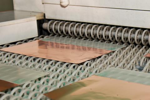
Production panels are chemically cleaned before applying photoresist. This step ensures proper adhesion of the circuit-forming film and removes contaminants that could interfere with imaging or etching.
- Conveyorized systems are used for consistent processing
- Thin core handling equipment protects ultra-thin materials
Circuit Pattern Exposure (Imaging)
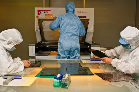
Photoresist-coated panels are aligned with circuit artwork and exposed to collimated UV light. This transfers the circuit image onto the panel surface.
- Both sides can be exposed simultaneously when required
- Imaging accuracy directly impacts final circuit definition
Etch Process
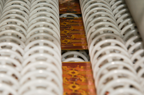
Chemical etching removes unwanted copper, leaving only the intended circuit pattern.
- Conveyorized systems ensure controlled material removal
- Thin core handling minimizes deformation
- Dual-sided etching is supported when needed
Drilling Process
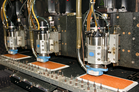
High-speed, high-precision drilling systems create holes for vias and interconnections.
- Mechanical drilling supports small hole patterns
- Laser drilling is available for ultra-small features
- Accuracy is critical for layer-to-layer connectivity
Copper Plating Process
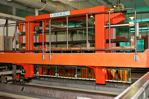
Electrolytic copper plating builds conductive pathways within drilled holes to establish electrical interconnects between layers.
- Fully automated systems ensure consistent deposition
- Enables reliable plated through-hole connections
Coverlay Application
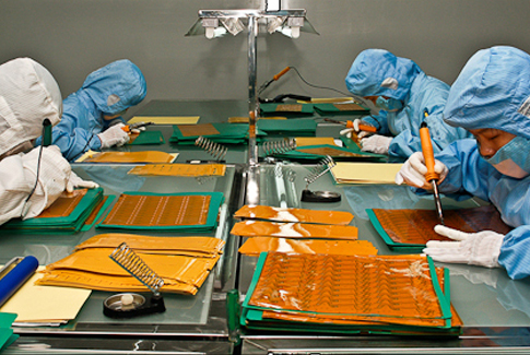
Polyimide coverlays are aligned and tacked into position prior to lamination.
- Provides insulation and environmental protection
- Ensures proper positioning before bonding
Coverlay Lamination
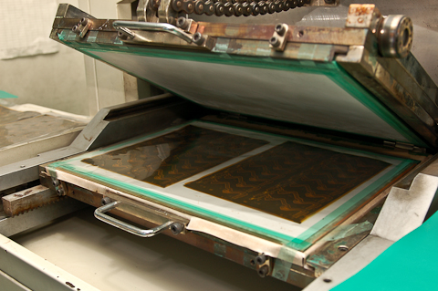
Coverlays are laminated using heat, pressure, and vacuum to ensure strong adhesion to the circuit.
- Controlled conditions prevent voids or delamination
- Maintains flexibility while protecting circuitry
Stiffener Application
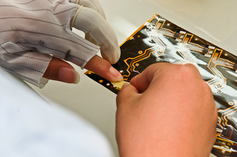
Localized stiffeners are added where required by design to reinforce specific areas of the circuit.
- Applied prior to lamination using heat and pressure
- Used to support connectors or component areas
- Maintains flexibility in other regions
Electrical Test
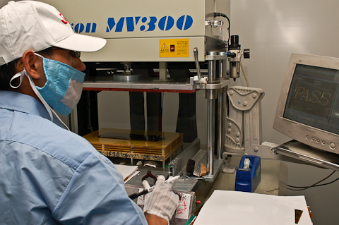
All circuits undergo 100% netlist-driven electrical testing per IPC-ET-652.
- Continuity and isolation are verified
- Grid and flying probe systems are used
- Simultaneous circuit testing ensures full coverage
Final Fabrication
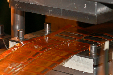
Individual parts are separated from production panels using precision cutting methods.
- Punch and die systems
- Laser cutting
- Mechanical routing
- Steel rule or chemically milled dies
Method selection depends on design requirements and geometry.
Key Manufacturing Phases
- Material Selection and Preparation - Material selection defines the foundation of circuit performance. Polyimide films, copper foils, and adhesives are chosen based on durability, flexibility, and compliance with industry standards.
- Imaging and Etching - The imaging process transfers circuit patterns using photoresist and UV exposure, followed by etching to remove excess copper. This phase determines circuit precision and feature definition.
- Drilling and Plating - Drilled vias and holes are plated to form conductive interconnections between layers, enabling reliable electrical pathways throughout the design.
Coverlay and Surface Protection
Coverlays protect exposed copper and support long-term durability. Surface finishes such as ENIG provide a solderable, oxidation-resistant interface for assembly.
Technical Specifications and Standards
Key Specifications:
- Minimum Bend Radius: Defines how tightly the circuit can flex without damage
- Maximum Layer Count: Determines design complexity and routing capability
- Temperature Range: Establishes operating limits for environmental reliability
Additional Performance Attributes:
- Flexibility: Supports repeated flexing in dynamic applications
- Thickness Options: Available to match mechanical and design constraints
- Electrical Conductivity: Ensures consistent signal and power transmission
Compliance and Testing:
Flex and rigid-flex circuits are built and verified to recognized industry standards, including:
- IPC-6013 for flexible circuit performance and qualification
- IPC-2223 for flex circuit design practices
- MIL-P-50884 for military-grade requirements
Testing includes electrical validation, as well as thermal and mechanical stress evaluations to ensure durability across application environments.
Frequently Asked Questions
Quick Links
- What is the manufacturing process for flex circuits?
- What happens during the imaging process?
- Why is polyimide used in flex circuits?
- What role do stiffeners play in flex circuits?
- Which specifications matter most in flex design?
- How are flex circuits tested for quality?
- What protects the circuits after fabrication?
What is the manufacturing process for flex circuits?
The process includes material preparation, imaging, etching, drilling, plating, coverlay application, lamination, stiffener placement, electrical testing, and final fabrication. Each step is controlled to protect thin materials and ensure circuit accuracy.
What happens during the imaging process?
Photoresist is applied to the substrate and exposed to UV light through circuit artwork. This transfers the circuit pattern to the panel before etching removes unwanted copper.
Why is polyimide used in flex circuits?
Polyimide films are selected for their durability and flexibility, allowing the circuit to bend and perform reliably under mechanical stress and varying environmental conditions.
What role do stiffeners play in flex circuits?
Stiffeners are applied to specific areas where additional mechanical support is required, such as connector regions. They reinforce localized sections without compromising overall flexibility.
Which specifications matter most in flex design?
Key specifications include minimum bend radius, maximum layer count, and operating temperature range. These directly impact performance, reliability, and application suitability.
How are flex circuits tested for quality?
All circuits undergo 100% electrical testing using netlist-driven methods to verify continuity and isolation. Additional testing includes thermal and mechanical stress validation.
What protects the circuits after fabrication?
Polyimide coverlays are laminated over the circuitry to protect against environmental exposure, while surface finishes improve solderability and prevent oxidation.
Start Your Flex Circuit Project
If you need guidance on flex or rigid-flex manufacturing requirements, Epec can help you evaluate your design and deliver a solution aligned with your performance and reliability goals.
Request a Quote Request Design Support Request More InformationRequest a FREE Quote!
We are here to help you with all your rigid-flex PCB needs.
Get Your Quote Now! Not Ready for a Quote? Request more info or email us your inquiry.Ebook - Designing Flex Circuits for Dynamic Bending Applications
 Download Your Copy
... Or Download Our Flex & Rigid-Flex Circuits Design Guide
Free DFM File Check

Submit your flex or rigid-flex PCB data files and we will run a complete DFM check for manufacturability.
Submit Your Data