



Common Flex & Rigid-Flex Circuit Board Material Stack-Up
Below you will find various flex and rigid-flex PCB stack-ups ranging from 4-layers all the way up to 12-layers. With these stack-ups, we can support a wide variety of alternatives, from single to multiple airgaps, uneven flex layer counts, and a singular flex section.
Beyond this, we can also support rigid-flex stack-ups all the way up to 18-layers. For stick-up questions, requests, and feedback, feel free to contact us and we will refer you to our flexible circuits product manager to assist in creating the stack-up that best suits your design needs.
If you are looking for more information about flex circuit construction methods, we recommend seeing our technical article on the latest material and construction methods provide the highest quality rigid-flex PCBs.
At a Glance: Flexible PCB Material Stack-Up
- Common flex and rigid-flex PCB stack-ups range from simple 1-layer flex circuits to complex 12+ layer rigid-flex constructions, supporting a wide variety of mechanical and electrical design requirements.
- Stack-up design directly impacts reliability, flexibility, impedance control, bend performance, thickness, and overall manufacturability of the finished circuit.
- Epec's engineering team provides DFM reviews and stack-up guidance to help optimize material selection, layer construction, and long-term product performance.
Free DFM and Stack-Up
Send us your flex or rigid-flex PCB data files and our engineering team will perform a complete DFM and help you create your stack-up.
Use the links below to jump to an example.
- 1 Layer Flex PCB Stack-up with Optional FR-4 Stiffeners and PSA
- 2 Layer Flex Circuit Stack-up with ZIF Contact Fingers
- 6 Layer Flex Circuit Stack-up
- 8 Layer Flex Circuit Stack-up
- 4 Layer Rigid-Flex PCB Stack-up (2 Flex Layers)
- 6 Layer Rigid-Flex PCB (with Air Gap)
- 8 Layer Rigid-Flex PCB
- 10 Layer Rigid-Flex PCB
- 12 Layer Rigid-Flex PCB (with Air Gap)
Flex PCB Stack-up Examples
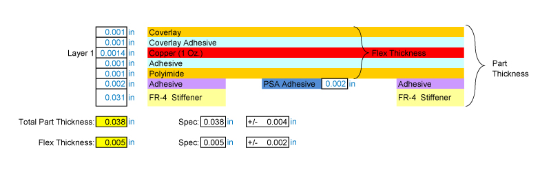
1 Layer Flex PCB Stack-up with Optional FR-4 Stiffeners and PSA
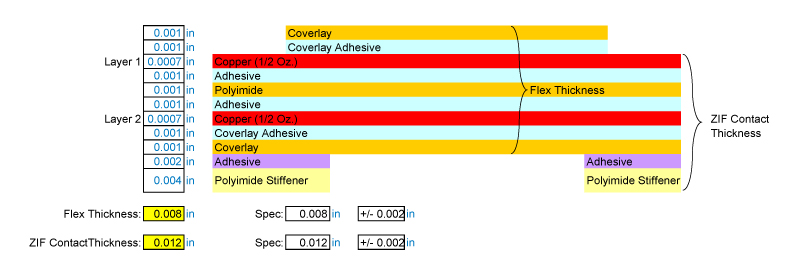
2 Layer Flex Circuit Stack-up with ZIF Contact Fingers
6 Layer Flex Circuit Stack-up

8 Layer Flex Circuit Stack-up

Rigid-Flex PCB Stack-up Examples
4 Layer Rigid-Flex PCB Stack-up (2 Flex Layers)
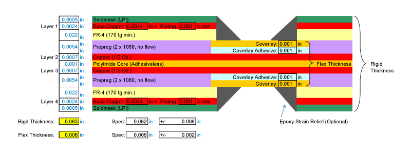
6 Layer Rigid-Flex PCB (with Air Gap)

8 Layer Rigid-Flex PCB

10 Layer Rigid-Flex PCB

12 Layer Rigid-Flex PCB (with Air Gap)

See our blog post on common flex and rigid-flex PCB constructions for additional stack-ups from 2-12 layers.
Watch Our Video
Designing Flex and Rigid Flex PCB Stack-Ups with Advanced Software
See our in-depth tutorial on creating a stack-up using our advanced software! In this video, we walk you through the process of generating a new stack-up, starting with the default settings and customizing it to fit your specific requirements.
Additional Resources
Below you will find related resources on flex circuit materials.
- Flex PCB Stack-up Documentation
- Defining Stack-Ups for Flex and Rigid-Flex Circuit Boards
- Defining Stack-Ups for Flex and Rigid-Flex Circuit Boards – Q&A
- Rigid-Flex PCB Stack-ups for Impedance Controlled Designs
- Using Adhesives and Bonding in Flex or Rigid-Flex PCB Construction
- How Rigid-Flex PCB Design Configurations are Advancing
Frequently Asked Questions
Quick Links
- What is a flex or rigid-flex PCB stack-up?
- How many layers can flex and rigid-flex circuit boards support?
- Why is stack-up design so important in flex and rigid-flex PCBs?
- What are air gaps and when are they used in rigid-flex designs?
- How can a DFM review improve a flex or rigid-flex PCB stack-up?
What is a flex or rigid-flex PCB stack-up?
A stack-up is the detailed construction blueprint of a flex or rigid-flex circuit board. It defines the arrangement of conductive layers, dielectric materials, coverlays, adhesives, stiffeners, air gaps, and rigid sections throughout the design. The stack-up serves as the foundation for manufacturing and plays a critical role in determining the circuit's electrical performance, flexibility, thickness, and reliability.
How many layers can flex and rigid-flex circuit boards support?
Flex circuits can be manufactured in configurations ranging from simple single-layer designs to complex multilayer constructions. Rigid-flex PCB stack-ups commonly range from 4 to 12 layers, with support for designs up to 18 layers depending on the application's requirements. More complex stack-ups can incorporate multiple flex regions, air gaps, uneven flex layer counts, and specialized rigid-flex transitions to meet challenging mechanical and electrical design goals.
Why is stack-up design so important in flex and rigid-flex PCBs?
The stack-up directly influences how the circuit behaves mechanically and electrically throughout its life cycle. Material selection, copper distribution, layer arrangement, and flex region construction all affect bend reliability, controlled impedance performance, signal integrity, thermal behavior, and manufacturability. A properly engineered stack-up helps reduce stress concentrations, improve durability, and prevent failures caused by repeated flexing or environmental conditions.
What are air gaps and when are they used in rigid-flex designs?
Air gaps are intentionally created spaces between layers in specific areas of a rigid-flex construction. They are often used to improve flexibility, reduce bending stress, and enhance the mechanical performance of dynamic flex regions. By allowing portions of the flexible circuit to move more freely, air gap constructions can improve long-term reliability in applications that experience repeated bending or flexing during operation.
How can a DFM review improve a flex or rigid-flex PCB stack-up?
A Design for Manufacturability (DFM) review allows engineers to evaluate the proposed stack-up for potential manufacturing, reliability, and cost concerns before production begins. During the review, factors such as layer count, material choices, bend areas, impedance requirements, stiffener strategy, and overall construction are examined. Addressing these considerations early helps reduce redesigns, improve manufacturing yields, and ensure the final stack-up is optimized for both performance and production.
Optimize Your Project with Epec's Expert Advice
Engage our engineering team for the best material stack-ups for flex and rigid-flex PCBs. Simply request your custom quote today for top-quality construction solutions.
Request a Quote Request Design Support Request More InformationRequest a FREE Quote!
We are here to help you with all your rigid-flex PCB needs.
Get Your Quote Now! Not Ready for a Quote? Request more info or email us your inquiry.Ebook - Designing Flex Circuits for Dynamic Bending Applications
 Download Your Copy
... Or Download Our Flex & Rigid-Flex Circuits Design Guide
Free DFM File Check

Submit your flex or rigid-flex PCB data files and we will run a complete DFM check for manufacturability.
Submit Your Data