Wave Soldering Defects
Pin Holes & Blow Holes on a Printed Circuit Board
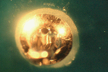
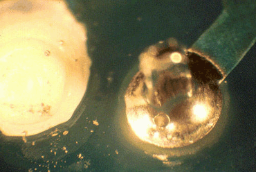
Pin holes or blow holes are the same thing and caused by the printed board outgassing during soldering. Pin and blow hole formation during wave soldering is normally always associated with thickness of copper plating. Moisture in the board escapes through either thin copper plating or voids in the plating. The plating in the through hole should be a minimum of 25um to stop the moisture in the board turning to water vapor and gassing through the copper wall during wave soldering.
The term pin or blow hole are normally used to indicate the size of the hole, pin being small. The size is solely dependent on the volume of water vapor escaping and the point the solder solidifies.

Figure 1: Blow Hole
The only way to eliminate the problem is improve the board quality with a minimum of 25um of copper plating in the through hole. Baking is often used to eliminate the gassing problems by drying out the board. Baking the board takes the water out of the board, but it does not solve the root cause of the problem.

Figure 2: Pin Hole
Nondestructive Evaluation of PCB Holes
The test is used to evaluate printed circuit boards with plated through holes for outgassing. It indicates the incidence of thin plating or voids present in through hole connections. It may be used at goods receipt, during production or on final assemblies to determine the cause of voids in solder fillets. Provided that care is taken during testing the boards may be used in production after test without any detriment to the visual appearance or the reliability of the final product.
Test Equipment
- Sample printed circuit boards for evaluation
- Canada Bolson oil or a suitable alternative that is optically clear for visual inspection and can be easily removed after test
- Hypodermic syringe for application of oil in each hole
- Blotting paper for removing excess oil
- Microscope with top and underside lighting. Alternatively, a suitable magnification aid of between 5 to 25x magnification and a light box
- Soldering iron with temperature control
Test Method
- A sample board or part of a board is selected for examination. Using a hypodermic syringe, fill each of the holes for examination with optically clear oil. For effective examination, it is necessary for the oil to form a concave meniscus on the surface of the hole. The concave form allows an optical view of the complete plated through hole. The easy method of forming a concave meniscus on the surface and removing excess oil is to use blotting paper. In the case of any air entrapment being present in the hole, further oil is applied until a clear view of the complete internal surface is obtained.
- The sample board is mounted over a light source; this allows illumination of the plating through the hole. A simple light box or illuminated bottom stage on a microscope may provide suitable lighting. A suitable optical viewing aid will be required to examine the hole during test. For general examination, 5X magnification will allow viewing of bubble formation; for a more detailed examination of the through hole, 25X magnification should be used.
- Next, reflow the solder in the plated through holes. This also locally heats the surrounding board area. The easiest way to do this is to apply a fine-tipped soldering iron to the pad area on the board or to a track connecting to the pad area. The tip temperature can be varied, but 500°F is normally satisfactory. The hole should be examined simultaneously during application of the soldering iron.
- Seconds after the complete reflow of the tin lead plating in the through hole, bubbles will be seen emanating from any thin or porous area in the through plating. Outgassing is seen as a constant stream of bubbles, which indicates pin holes, cracks, voids or thin plating. Generally if outgassing is seen, it will continue for a considerable time; in most cases it will continue until the heat source is removed. This may continue for 1-2 minutes; in these cases the heat may cause discoloration of the board material. Generally, assessment can be made within 30 seconds of application of heat to the circuit.
- After testing, the board may be cleaned in a suitable solvent to remove the oil used during the test procedure. The test allows fast and effective examination of the surface of the copper or tin/lead plating. The test may be used on through holes with non tin/lead surfaces; in the cases of other organic coatings, any bubbling due to the coatings will cease within a few seconds. The test also provides the opportunity to record the results both on video or film for future discussion.
For more information see our blog post titled "What Is The Reason For Circuit Board Blow Holes?".


