



PCB Manufacturing Process Capabilities
Printed circuit board technologies have changed rapidly over the past several years, pushing capabilities of standard production facilities and limiting what you can build and where you can build it. New technologies require new production equipment.
Providing quality PCB parts in a single standard production house is a thing of the past. Not all circuit board parts fit into one location. Knowing the capabilities within your supply chain and expanding your offering is not only an investment but necessary for survival in the PCB world. As more PCB manufacturing companies close domestically and across the world, a strong, reliable company with history is what you need.
At a Glance: PCB Manufacturing Process Capabilities
- Advanced PCB manufacturing capabilities support high-density, high-reliability designs through technologies such as microvias, controlled impedance structures, fine-line circuitry, heavy copper construction, and multilayer registration control.
- Manufacturing capability limits directly influence circuit board design decisions involving drill sizes, aspect ratios, copper weights, line widths, layer counts, solder mask features, and impedance requirements.
- Understanding a manufacturer's process capabilities early in the design cycle helps reduce redesign risk and ensures the PCB can be produced consistently, cost-effectively, and to specification.
Below you will find a list of PCB manufacturing process capabilities.
| Category | Description | Sym. | Capability |
|---|---|---|---|
1. Microvia Diameter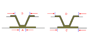 |
1.1 Microvia Diameter at Target Land |
A | 100 um 0.004" |
| 1.2 Microvia Diameter at Capture Land |
B | 125 um 0.005" |
|
| 1.3 Microvia Target Land Size |
C | 0.012" | |
| 1.4 Microvia Target Land Size |
D | 450 um 0.0177" |
|
2. Stagger & Stack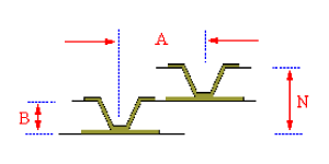 |
2.1 Min. Staggered Via Pitch Staggered Via Pitch |
A | 560 um 0.022" |
| 2.2 RCC Thickness RCC |
B | 50 um 0.002" |
|
| 2.3 Blind Via Layers |
N | 2 | |
3. Material & Construction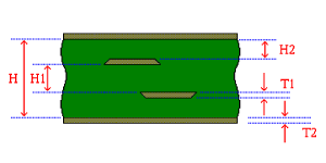 |
3.1 Finished Board Thickness |
H | 0.012" – 0.250" |
| 3.2 Min. Inner Layer Thickness |
H1 | 0.075 mm 0.003" |
|
| 3.3 Min. Dielectric Thickness |
H2 | 0.05 mm 0.002" |
|
| 3.4 Max. Inner Layer Copper |
T1 | 6 oz | |
| 3.5 Max. Outer Layer Copper |
T2 | 6 oz | |
4. Warp |
4.1 Warp & Twist (Max.) |
A B | < 0.75% |
5. Pad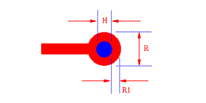 |
5.1 Min. Finish Hole Size |
H | 0.005" |
| 5.2 Min. Land Size |
H | 0.018" | |
| 5.3 Min. Annual Ring for Via |
R1 | IPC Class 2 | |
| 5.4 Min. Annual Ring for Component |
R1 | 0.05 mm 0.002", provided designed per IPC |
|
6. Drill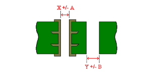 |
6.1 Tolerance for PTH Hole |
A | 0.08 mm 0.003" |
| 6.2 NPTH Hole Tolerance |
B | 0.05 mm 0.002" |
|
7. Registration for S/M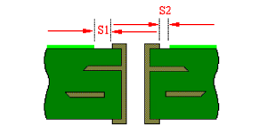 |
7.1 Registration for S/M to Pattern |
S1-S2 | 0.0024" |
| 7.2 Registration for Legend to S/M |
NA | 0.005" | |
8. Registration for Drill |
8.1 Registration for Drill to Inner Layer |
S | 0.075 mm 0.003" |
| 8.2 Registration for Drill to Datum |
S | 0.05 mm 0.002" |
|
| 8.3 Registration for First Drill to Second Drill |
NA | 0.005" | |
9. Registration for Layers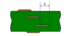 |
9.1 Layer to Layer for 4 layers |
S | 0.08 mm 0.003" |
| 9.2 Layer to Layer for 6 layers |
S | 0.10 mm 0.004" |
|
| 9.3 Layer to Layer for 8 layers |
S | 0.13 mm 0.005" |
|
10. Line Width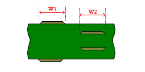 |
10.1 I/L Min. Width (0.5 oz) |
W2 | 0.003" |
| 10.2 O/L Min. Width (0.5 oz) |
W1 | 0.003" | |
11. Line Space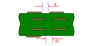 |
11.1 I/L Min. Space |
S2 | 0.003" |
| 11.2 O/L Min. Space (0.5 oz) |
S | 0.003" | |
12. Drill Capability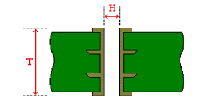 |
12.1 Max. Aspect Ratio (Board Thickness 0.063") |
H/T | 12.0 |
| 12.2 Min. Drill Hole Size (Board Thickness 0.063", After Plating) |
H | 0.0083 | |
13. S/M Thickness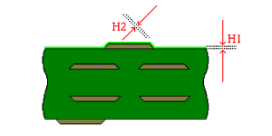 |
13.1 Max. Thickness on Copper |
H1 | 0.025 mm 0.001" |
| 13.2 Max. Thickness at Shoulder |
H2 | 0.0075 mm 0.0003" |
|
14. S/M Capability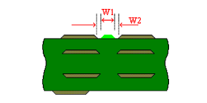 |
14.1 Min. SMD Space for Dam |
W2 | 0.0078" |
| 14.2 Min. Dam Size |
W1 | 0.004" 0.005" for white and black colors |
|
15. Carbon Capability |
15.1 Max. Contact Resistance |
NA | 30 Ω / sq |
| 15.2 Max. Primary Resistance |
NA | 30 Ω | |
| 15.3 Min. Thickness |
NA | 0.0004" | |
| 15.4 Min. Space |
A | 0.015" | |
| 15.5 Max. Space for Registration |
B | 0.007" | |
16. HAL Capability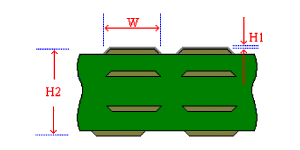 |
16.1 Min. PCB Thickness for HAL |
H2 | 0.6 mm 0.0236" |
| 16.2 Min. Pad Width/Space for HAL |
W | 0.25 mm 0.0098" |
|
| 16.3 HAL Thickness for any point |
H1 | 0.001 mm ~ 0.025 mm 40micro-inch ~0.001" |
|
| 16.4 Thickness on QFP Pad (0.05" Wide Quad) |
A | 0.015 mm ~ 0.030 mm 0.0006" ~0.0012" |
|
17. HAL Capability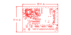 |
17.1 Outline Tolerance-Punching |
AB | NA |
| 17.2 Outline Tolerance-Routing |
AB | 0.005" | |
18. Beveling Capability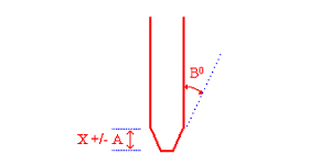 |
18.1 Beveling Angle |
B | 200-600 |
| 18.2 Tolerance for Outline of Bevel |
A | + - 0.005" | |
19. V-Cut Capability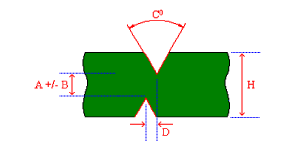 |
19.1 V-Cut Angle V-Cut |
C | 30° |
| 19.2 Range of Board Thickness |
H | 0.030"~0.125" | |
| 19.3 Tolerance of V-Cut Residual |
B | 0.05 mm 0.003" |
|
| 19.4 V-Cut Off Line V-Cut |
D | 0.125 mm 0.005" |
|
20. Test Capability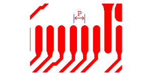 |
20.1 Voltage |
NA | 5 –500 VDC |
| 20.2 Isolation |
NA | 500 MΩ | |
| 20.3 Continuity |
NA | 20Ω~100KΩ | |
| 20.4 Min. SMD PAD Pitch SMD |
P | 0.3 mm 0.0118" |
|
21. Impedance Control Capability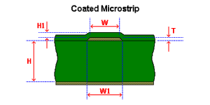 |
21.1 Impedance Control > 50O |
NA | +/- 10% |
| 21.2 Impedance Control < 50O |
NA | +/- 10% | |
22. Differential Impedance Capability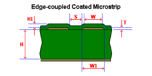 |
22.1 Differential Impedance Control > 50O |
NA | +/- 10% |
| 22.2 Differential Impedance Control < 50O |
NA | +/- 10% | |
| 23. Coplanar Impedance Capability |
22.1 Coplanar Impedance Control > 50O |
NA | +/- 10% |
| 22.2 Coplanar Impedance Control < 50O |
NA | +/- 10% |
Frequently Asked Questions
Quick Links
- Why are PCB manufacturing capabilities important during the design phase?
- What are microvias, and why are they used?
- What is controlled impedance, and when is it required?
- When should heavy copper PCB construction be considered?
- What manufacturing specifications should engineers review before finalizing a PCB design?
Why are PCB manufacturing capabilities important during the design phase?
Manufacturing capabilities establish the practical limits of what can be produced, including trace widths, spacing, hole sizes, layer registration, board thickness, copper weights, and impedance tolerances. Designing within these limits helps ensure manufacturability, yield, reliability, and cost control.
What are microvias, and why are they used?
Microvias are small laser-drilled interconnections used in high-density PCB designs to connect layers while minimizing space requirements. They support advanced packaging technologies, increased routing density, and more compact electronic assemblies.
What is controlled impedance, and when is it required?
Controlled impedance is the ability to manufacture PCB traces to a specified impedance value within a defined tolerance. It is commonly required for high-speed digital, RF, and communications applications where signal integrity is critical.
When should heavy copper PCB construction be considered?
Heavy copper designs are typically used in applications that require higher current-carrying capacity, improved thermal performance, or increased power-handling capability. The source identifies support for copper weights up to 6 oz on both inner and outer layers.
What manufacturing specifications should engineers review before finalizing a PCB design?
Engineers should evaluate capabilities related to microvias, drill sizes, aspect ratios, line widths and spacing, copper thickness, board thickness, solder mask tolerances, layer registration, impedance control, routing tolerances, and testing requirements to ensure the design aligns with manufacturing limits.
Need An Advanced PCB Design Manufactured?
Upgrade your PCB production with our advanced capabilities. Stay ahead with precision and reliability. Get your custom quote now!
Request a Quote Request Design Support Request More InformationRequest a FREE Quote!
We are here to help you with all your printed circuit board needs.
Get Your Quote Now! Not Ready for a Quote? Request more info or email us your inquiry.FREE Download: 10 Key Factors Behind HDI PCB Performance
 Download Your Copy
... Or Download Our Circuit Board Design Guide
Free DFM File Check

Submit your PCB data files and we will run a complete DFM check for manufacturability.
Submit Your Data