PCB Data Requirements & Fabrication Instructions
Below you will find the minimum data information requirements needed to place your rigid circuit board order. The purpose of this web page is to describe the minimum data and information required to generate the tooling for your printed circuit board.
The minimum required data and information set can be broken down into two categories: "Printed Circuit Board Data" and "Printed Circuit Board Fabrication Instructions".
Printed Circuit Board Data
Printed Circuit Board data shall consist of the follow information to expedite your order into production without delays.
Gerber Data (In the following formats):
- RS274D including separate aperture list with all apertures defined. (All apertures that are not defined, the data cannot be processed and may need manual edits leading to a risk of error and delays into production.)
- RS274X – Preferred – embedded apertures included
- Gerber files with aperture lists (a complete list is needed including all d-codes)
- DXF in some cases can be used; this format always requires an approval once data has been converted to RS274X format prior to production. Engineering will work with you to review in Gerber or PDF format.
- ODB++ format, this file format is typically large and can be difficult to transfer via email. Setting up a share file location may be needed for safe transfer of files. ODB++ will be supplied as a single file, usually with the extension of .tgz. ODB++ contains all the required board and drill information.
Drill Data (In the following formats):
- Excellon 1
- Excellon 2
Note: Any other data formats need to be reviewed and approved by Epec Engineered Technologies before the order can be placed into production.

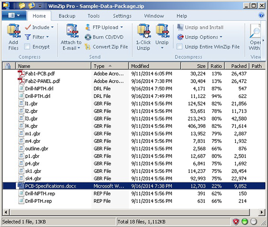
Example of a Complete PCB Data Package
Netlist Data:
Supplying a NETLIST is not required but recommended with all PCB requirements.
A netlist is critical to comparing the generated data base to the electrical properties desired. When comparing Gerber data to a netlist, the netlist will report all discrepancies. Our engineer team will report all issues found within the data typically leading to an additional revision of the data. The netlist will confirm the design matches or fails for shorts or opens. When used properly a netlist is vital to producing quality product for production files and electrical test. Ask your printed circuit board designer to always include netlist data, preferably IPC-356 format. Netlist is in an ASCII format and should be readily available.
See our blog post on PCB Fabrication Data File Requirements for more information.
Printed Circuit Board Fabrication Instructions
The fabrication instructions or notations should be clearly presented at the quote request and contain all relevant information required to tool and build the part. The following list is the minimal information to prevent delays in engineering:
Slot and Hole Sizes:
- Slot and Hole Sizes:
Board Outline:
- Board outline and details with all required dimensions and tolerances. A 1:1 with actual PCB size, shape and cutouts to develop a clear routing program for your printed circuit board profile. Supplying an accurate outline allows engineering to add dimensions where needed for key processing elements.
- Hole or feature to edge dimensions, X , Y coordinates. Supplying a hole to PCB edge shows the exact placement of the drills within the PCB outline.
Finished Copper Weights:
- Finished Copper Weights for all copper layers internal and external. Specifying finished copper is critical to production and cost for build.
- Balancing the copper from side to side on internal layer construction allows for ease of production. Example: a 4-layer PCB that uses a single core for layer 2 – 3 each layer when possible should have the same copper weight. Matching copper weights will cut down on lead time and at times can save cost.
Finished Board Thickness:
- Finished Board thickness with tolerances and measurement criteria.
- +\-10% is industry standard for final measurements, an 0.062 mils +\- 0.006 mils for example would finish between 0.056 mils - 0.068 mils
- Where the PCB is to be measured for final thickness is seldom specified but can make a difference in final applications. When thickness is critical, specify for final inspection where to measure the PCB. Over Metal, Over Mask, Over Laminate, or over a combination of these sets the process of selecting materials to be used in construction of the stack-up.
Surface Finish:
Surface finish preference – Non-RoHS or RoHS compliant.
- HASL - Hot Air Solder Level - contains LEAD non-RoHS
- ENIG - Electroless Nickel Immersion Gold - the most popular finish
- Immersion Silver – RoHS compliant will tarnish like any silver product
- OSP – Organic Solder ability Preservative
- LF-HASL - Lead Free Hot Air Solder Level
- Immersion Tin - used the least of all finishes
Soldermask Requirements:
Soldermask requirements state the color desired, almost any color can be achieved in PCB finish however sticking to basics are best in a Gloss finish. The most popular are:
- Green
- Blue
- White
- Red
For additional colors this will require an engineering review, availability and possible Minimum Order Quantity (MOQ) charges. Ask if you have special requirements that need to be met.
Mask can be in either Matte or Gloss in the 4 basic color selections – expect added time to process for specific textures for specific colors. Matte is less readily available due to Gloss is most widely used. Processing Matte for certain colors may add time due to equipment change over, processing clean up and application.
Silkscreen Requirements:
Silkscreen requirements state the desired color desired on the PCB, most are UV cured inks and are RoHS compliant.
- White
- Yellow
- Black
Those are the most widely used colors; others are available however, like MASK, colors can add to process time and cost. Ask if you have special requirements for your product.
Technical Contact Information:
Any time a NEW or a NEW REVISION part is brought into process there can be technical questions from engineering or production. Supplying a technical contact is vital to minimizing time loss. An email addresses and phone line will help us move quickly to get your order back into process. Epec unlike most of our competition operates on a 24/7 production schedule alternate contacts for nights and weekends is also advantageous in preventing delays.
Additional Requirements:
Any additional requirements (i.e. impedance, controlled dielectrics, plugged vias, via in pad process, (blind and buried vias) selective surface finishes, counter bores, counter sinks, milling, etc. all should be noted on fabrication drawings for processing.)
Fabrication Instructions:
The fabrication instructions should be provided in a clean legible format, supplying a Gerber format of the fabrication drawing is always best for engineering. Other formats can be used such as:
- Adobe Acrobat (.pdf)
- Gerber
- RS274X
- HPGL
- AutoCAD (.dwg or .dxf)
- Graphic file (.jpg, .gif, .tif, etc.)
- ODB++
Array / Panel Configurations: An array is a grouping of like parts with the same attributes build and linked through waste material to be assembled within the grouping.
- Specify the preferred method, scored or tab routed. In some cases a combination of both are used.
- Score details – desired web and depth are best left to engineering. When heavy components may be used providing score details will prevent assembly issues.
- Tab routing – location of tabs and keeping copper .020 away from the PCB edges will ease manufacturing issues.
- Fiducial locations, shapes and size can be placed on waste rails or within each printed circuit board when spacing allows.
- Typical fiducial used 0.050 mils - 0.060 mils 3 locations per side needing component placement.
- 0.100 mils diameter mask clearances will be added to mask layers
- Adding donut shaped copper around the fiducial in the waste are will preserve the fiducial during process. The donut shape will be covered with mask on the delivered goods.
Both score details and tab rout details hinge on the Tg of materials, thicknesses and positioning of copper. Engineering assistance is available through our free DFM service.
See our blog post on Creating Standard PCB Fabrication Notes for more information.
Ready To Take Your PCB Project From Concept to Production?
Ensure a smooth, delay-free production process by providing us with the required printed circuit board data and fabrication instructions. Get started and make your project a success with Epec Engineered Technologies.
Request a Quote Request Design Support Request More Information


