Controlled Impedance Designs
Controlled impedance PCB designs address signal integrity challenges created by fast edge rates and high clock speeds by treating traces as transmission lines rather than simple connections. Epec Engineered Technologies applies material control, imaging precision, and etch process control to manufacture printed circuit boards that meet specified impedance values and tolerances. This approach helps minimize reflections, noise, and performance degradation in high-speed digital circuitry.
At a Glance: Controlled Impedance Designs
- Addresses signal integrity challenges caused by faster switching speeds and shorter rise times in PCB designs.
- Treats PCB traces as transmission lines and tightly controls materials, imaging, and etching to meet specified impedance values and tolerances.
- Helps reduce reflections, noise, and performance degradation in high-speed digital circuits through disciplined manufacturing processes.
Controlled Impedance on Printed Circuit Boards
As signal switching speeds continue to increase, PCB designers must pay closer attention to the impedance characteristics of printed circuit board traces. Short transition times and high-frequency operation mean PCB traces behave like transmission lines, not ideal conductors. In this environment, the electrical properties of the trace geometry, materials, and reference planes directly influence circuit performance.
A useful way to visualize this is to think of a PCB trace as a precisely constructed cable. Similar to the center conductor of a coaxial cable, the trace carries the signal while the surrounding laminate insulates it from the return path, typically a ground plane. In many designs this relationship can be represented by a microstrip cross section.
Why Impedance Matters at High Speeds
As switching speeds rise, trace impedance becomes increasingly critical. Electrical impedance describes the opposition to time-varying current in a circuit. When a signal encounters a change in impedance caused by differences in geometry or materials, part of the signal is reflected while the remainder continues forward. These reflections can introduce distortions such as noise, reduced gain, or unpredictable errors that degrade overall system performance.
To reduce these effects, designers specify target impedance values with defined tolerances and rely on the PCB manufacturer to precisely meet those requirements.
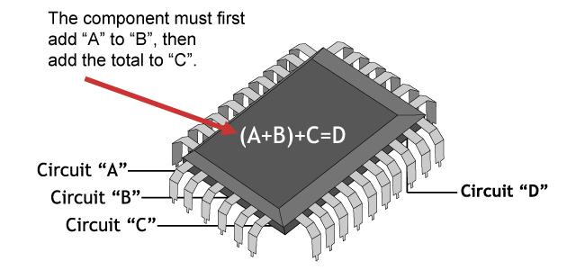
A Very Simple Example:
Consider three signals (A, B, and C) that arrive at a component at the same time. If signal C must be delayed so the component can first process the combined result of A and B, impedance can be intentionally applied to the C trace. By adjusting impedance, the signal is slowed just enough to maintain correct functional timing.

Designing for Increasing Impedance Requirements
As signal rise times continue to decrease, the number of traces requiring impedance control will naturally increase. Achieving accurate control depends on modeling impedance using a cross section that closely matches the finished board. This highlights the importance of consistent materials, precise imaging, and controlled etching throughout the manufacturing process.
Where Epec’s Experience Supports Impedance Control
With more than 70 years of PCB manufacturing experience, Epec Engineered Technologies has developed processes focused on maintaining tight impedance control from incoming materials through final fabrication.
Incoming Inspection and Vendor Material Management Process
Working closely with key suppliers, Epec has established controls to ensure incoming laminates, prepregs, and copper foils meet consistency requirements for thickness and other critical properties. Variations in raw material thickness are one of the primary challenges in producing boards with controlled impedance, making material management a foundational step.
Laser Direct Imaging (LDI) Equipment
Laser Direct Imaging reduces trace-width variation by eliminating film expansion and contraction. It also produces sharper, more defined copper images. This improved definition allows traces to etch with tighter dimensional control, which directly supports meeting specified impedance values.
Etch Equipment Configuration
After imaging, controlled impedance circuit boards enter the etching process. Key parameters, such as etch speed, temperature, pressure, and nozzle direction, must be configured to minimize copper undercut. Drawing on long-standing industry experience, Epec manages these variables to ensure the final trace geometry aligns with the customer’s impedance tolerance requirements.
Video Resources on Controlled Impedance
Epec also provides a video series covering major aspects of controlled impedance design and validation:
Part 1: Understanding the Stack-Up in Impedance Calculations
Part 2: Gerber Data
Part 3: Impedance Validation
These resources illustrate how design data, materials, and fabrication processes work together to achieve controlled impedance.
Additional Resources:
- How to Specify Your PCB Controlled Impedance Requirements
- A PCB Trick for Vias and Impedance Traces
- Understanding Impedance Control in PCB Manufacturing
- PCB Impedance Calculator
Frequently Asked Questions
Quick Links
- What is controlled impedance in PCB design?
- Why do PCB traces need impedance control at higher speeds?
- What causes signal reflections on a PCB trace?
- How do designers typically specify controlled impedance?
- Why is raw material consistency important for impedance control?
- How does LDI help with controlled impedance?
- What role does the etch process play in impedance accuracy?
What is controlled impedance in PCB design?
Controlled impedance refers to designing and manufacturing PCB traces so their electrical impedance stays within a specified value and tolerance, which is critical for high-speed signals.
Why do PCB traces need impedance control at higher speeds?
At high switching speeds, traces act like transmission lines. Without impedance control, reflections can occur and degrade signal quality.
What causes signal reflections on a PCB trace?
Reflections occur when a signal encounters changes in impedance due to variations in materials or trace geometry, causing part of the signal to reflect.
How do designers typically specify controlled impedance?
Designers define target impedance values and allowable tolerances for specific traces and rely on the PCB manufacturer to meet those specifications.
Why is raw material consistency important for impedance control?
Variations in laminate, prepreg, or copper thickness can significantly affect impedance, making consistent incoming materials essential.
How does LDI help with controlled impedance?
Laser Direct Imaging eliminates film-related width variation and produces more precise trace images, improving etch accuracy and impedance consistency.
What role does the etch process play in impedance accuracy?
Careful control of etch parameters minimizes undercut and helps ensure the final trace geometry meets the required impedance tolerance.
Does Your Design Have Tight Impedance Controls?
For designs requiring tight impedance tolerances, down to ±5%, Epec applies precision-controlled manufacturing processes to support signal integrity. By combining material consistency, advanced imaging, and controlled etching, Epec aims to meet or exceed customer-defined impedance requirements on high-speed PCB designs.
Trust Epec's 70+ years of expertise for unmatched accuracy. Request a quote now to ensure your design's success.
Request a Quote Request Design Support Request More Information


