Hybrid RF & Microwave Circuit Boards
A hybrid printed circuit board (PCB) multilayer is a PCB that uses dissimilar materials with the intent of optimizing electrical performance and improving system reliability focused towards high-frequency RF applications. The biggest challenge when manufacturing this type of PCB is managing the different coefficient of thermal expansion (CTE) properties of the dissimilar circuit materials both during PCB fabrication and component assembly.
Typically these designs include a combination of FR-4 material and PTFE laminates which allows a designer to condense both RF functionality and RF functionality on the same PCB which can reduce both the footprint of the device and the costs.
All of the world class laminate manufacturers like Isola, Rogers, Arlon, and Taconic all have published significant technical information on the properties and performance of their laminates. In the following sections we will point out some of the capabilities that we provide and some of the items to avoid when designing a RF Hybrid PCB circuit.
Our experience allows us to provide our customers with most comprehensive service in circuit board production for these products as we have invested in.
Laminate Construction Considerations for Hybrid RF PCBs
When producing a printed circuit board with dissimilar materials it is critically important to have experience in both the physical properties of the laminate and the capabilities of your equipment. Based upon the CTE values of all of the layers of material (ex FR4, PTFE, and Copper) each material grows at a different rate during elevated thermal exposure (i.e. lamination). This can cause significant registration issues as one material shrinks while another one expands and it can also cause delamination of the copper-to-substrate interfaces. Therefore, not all materials should be used in hybrid applications as they are not manufacturable regardless of the desired performance.
Working with your PCB fabricator early in the design process will give you the best results as they are most aware of what materials can work best together. For example, Rogers 5880 is a fantastic RF material used in high reliability applications. The biggest challenge with the material is that it contracts (shrinks) after you etch the copper off so a fabricator needs to understand how that works in their process to compensate for this issue.
Hybrid constructions typically involve a low loss material such as Nelco or Rogers combined with another core material like FR-4.
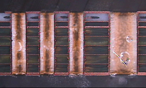
FR-4, Rogers, and Mixed Copper Hybrid PCB Construction
Stack Up Challenges for Hybrid Microwave PCBs
A major part of any RF/microwave application is the ability to stay within the specific tolerances of a design so that the required frequencies can be achieved. One of the most difficult challenges in managing the stack-up of a hybrid design is consistently achieving an overall thickness requirement from panel to panel and even piece to piece in some applications. Since there is more than one material type, there will also be more than one prepreg (adhesive system) type that can be used to laminate the design together.
A lot of RF designs have RF signal layers that have large open (un copper filled) areas after etching, a fabricator will use different techniques to assure that there is plenty of insulation between the layers and that we have a consistent overall thickness.
In many instances a no-flow FR-4 prepreg will be the best solution to keep the thickness uniform but that can add material to the overall stack up and change the electrical properties of the entire package. Not all PCB fabricators processes work exactly the same which is another reason why early involvement is critical to a successful design.
Unique Mechanical Features of High Frequency PCBs
While managing the electrical and RF properties of a Hybrid PCB is full of enough challenges, there are several unique mechanical features often desired by PCB designers that are difficult to put into cost effective manufacturing practices. A few specific items include:
Odd Shape Board Outlines
A lot of times these product must fit into unique enclosures or other space there are many times that the RF PCB outline has many different twists and turns. While routing the outline of a PCB is usually not that difficult, it is quite a sensitive process when dealing with a Hybrid design. Some of the PTFE materials are very soft, the feeds and speeds must be slowed down to make sure that the edges are crisp.
Another factor is that you must constantly monitor your drill bits as the material is much more aggressive on drill bits. This means that you can possibly get out of tolerance if the bit wears down too much during the process. The last thing to keep in mind is that most RF products are made of a woven type material which means that it will easily fray if it is not cut properly.
Controlled Depth Rout Patterns or Internal Pockets
The picture below illustrates what a complex RF Hybrid PCB design looks like with internal pockets. Some of these features can be manufactured using multiple lamination cycles while others must be done using a controlled depth routing process of some sort, usually a router bit or laser cutter. Both of these processes have specific challenges that can add cost and complexity to the hi-speed PCB design.
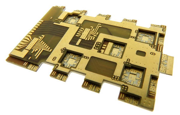
Complex RF Hybrid PCB design with internal pockets.
When using multiple lamination cycles to create these pockets or cavities a manufacturer is required to rout out the pattern in the production panel and in the prepreg. Once these patterns are complete then it is very critical that the registration of the patterns are spot on otherwise the bond will not pass IPC standards or you will have prepreg leakage where the prepreg comes out from between the layers and could cover a specific RF component of the board.
For applications that requires a controlled depth process, there is very little room for error as the amount of distance between the material that needs to be removed and the copper feature below it can be a little as 1 mil.
Plated Through Hole Consistency
Traditional hole preparation prior to plating for FR4 is not the same as PTFE. A fabricator must be aware of how there processes impacts the hole wall quality. For PTFE, the typical method used to “desmear” the holes prior to plating is by using plasma etch process. While this does a good job of preparing the hole wall of the PTFE, it can also react more aggressively to the FR4 and create an uneven surface which will then turn into uneven copper in the holes which can cause voids or electrical failure.
Another feature prevalent in RF/microwave PCBs is plugging vias, both internal and external with conductive material to dissipate heat. In order to have a consistent amount of material in each hole and to keep the RF properties in tolerance it is critical to ensure that holes are drilled, cleaned, and plated properly prior to filling.
Since all of the materials have different density and other characteristics, nothing beats experience in processing these types of parts.
Looking for a Hybrid PCB Solution?
Maximize the performance and reliability of your high-frequency RF applications with our expert hybrid PCB manufacturing. Get a quote today to take your RF design to the next level.
Request a Quote Request Design Support Request More Information

