High-Speed PCBs and 5G Technology Considerations and Challenges
By Ed McMahon, CEO
Epec Engineered Technologies
Should we say that fifth generation (5G) technology has arrived? Yes. More mobile wireless communication systems are upgrading and converting over their processes to adopt 5G technologies for better connectivity to the Internet of Things (IoT) (Figure 1). The dizzying speeds of 5G will open new market opportunities to all industries that will use, design, and manufacture the components and applications that will use these systems.
So, what does this mean to the high-speed PCB industry? Material considerations will be the top aspect that will have to be evaluated for designing and building the PCB stack-up. The 5G PCB will have to address all the specifications when carrying and receiving signal transmissions, providing electrical connections, and offering controls for specific functions. Also, challenges to the PCB design will need to be addressed, such as maintaining the signal integrity at those higher speeds, dealing with thermal management, and what to do to prevent electromagnetic interference (EMI) between digital and analog boards.

Figure 1: Depiction of 5G technologies for better connectivity.
Mixed Signal Acceptance Circuit Board Designs
Most systems now are handling 4G and 3G PCBs. This means that components are transmitting and receiving frequencies that can range from 600 MHz up to 5.925 GHz and bandwidth channels of 20MHz, or 200kHz for IoT systems. When designing PCBs for 5G network systems, the components will need Mm-wave frequencies of 28GHz, 30GHz, and even 77GHz based on the application. For bandwidth channels, 5G systems will be dealing with 100MHz right below and 400 MHz right above 6GHz frequencies.
These higher speeds and higher frequencies will demand the appropriate materials within the PCB to capture and transmit both lower and higher signals at the same time without experiencing signal loss and EMI. In addition, an added problem is that the devices will become lighter, portable, and smaller. With strict weight, size, and space limitations, the PCB materials will have to be flexible and light while accommodating all the microelectronics along the board.
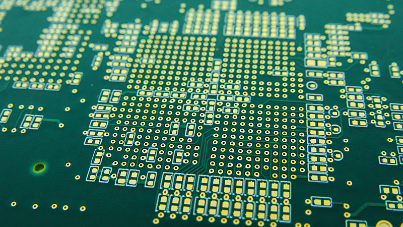
Thinner traces and stricter impedance control will need to be adhered to for the PCB copper tracings (Figure 2). The traditional subtractive etching processes used for 3G and 4G high-speed PCBs may be switched out for modified semi-additive processes. These modified semi-additive processes will provide more precise trace lines and straighter walls.

Figure 2: Printed circuit board designed with tight lines and spaces.
Material substrates are also being redesigned. Printed circuit board companies are looking at materials that provide a dielectric constant as low as 3, as standard materials for lower speed PCBs are usually 3.5 to 5.5. Tighter fiberglass weaves, lower dissipation factor loss materials, and low-profile copper will also be options for high-speed PCBs used for digital signals to prevent signal losses and to promote greater signal integrity.
EMI Shielding Challenges
EMI, cross talk, and parasitic capacitance are major problems with circuit boards. To deal with cross talk and EMI that will be present due to the analog and digital frequencies along the board, separating the traces is highly recommended. Using a multilayer board will offer greater versatility to decide on how to place the high-speed traces so the routes for both analog and digital return signals will be kept away from each other, while also keeping the AC and DC circuits apart. Adding shielding and filtering when arranging components should also lower the amount of natural EMI that will be present on the PCB.
To ensure that there are no defects on the surface of the copper as well as critical shorts or opens, advanced automated optical inspection systems (AIOs) and 2D metrology with greater functionality will be used more often to inspect the conductor's traces as well as to measure them. These technologies will help PCB fabricators look for possible signal degradation risks.
Thermal Management Challenges
Higher signal speeds will lead to higher generated heat from the electricity passing through the PCB. PCB materials used for the dielectric materials and the core substrate layers will need to adequately handle the high speeds required for 5G technology. If the materials are inadequate, copper trace peeling, delamination, shrinking, and warping can result as the problems can cause deterioration to the PCB.
To deal with these higher temperatures, fabricators will need to focus on material selections that address thermal conductivity and thermal coefficients. A material offering higher thermal conductivity, excellent heat transfer and consistent dielectric constants will be necessary to create a good PCB that will provide all the 5G functions that will be required for the application.
Creating the Right PCB Design
With the advent of 5G technology, printed circuit boards will be designed to offer the optimal signal integrity, impedance control, and thermal management. Due to the range of application specifications, designing the PCB will require working with a fabricator that has the knowledge and experience to work with the specific material requirements while also adhering to FCC requirements.
Customers will also have to consider when to start making the switch over to 5G based on their operations and applications. Some industries will have no choice but to fully accept 5G technology quickly to stay competitive in their market segment. Other industries may wish to take their time while considering the increased costs that are still present when selecting high-speed materials for the PCB stack-ups.
Adopting and leveraging the new technology, while keeping PCB scope creep low to control costs, will be a delicate balancing act. However, as the 5G technology becomes more mainstream, advanced techniques, materials, and fabrication equipment will be created to provide fabricators with greater capabilities to meet the high-speed PCB design and manufacturing demand. These technologies will also provide a more competitive field so that customers can find the right PCB design services that will meet their budgets.
Summary
Here at Epec Engineered Technologies, we offer customized build-to-print manufacturing capabilities to customers in a broad range of industry sectors, and 5G technology requires that circuit board manufacturers continue to invest in equipment and improved processing to be able to consistently deliver PCBs for this demanding application.
Looking for a High-Speed Circuit Board?
Our engineering team is here to help you with all your high-speed circuit board challenges. With over 70 years in the PCB industry, we have helped countless companies solve their high technology PCB challenges.
Request a Quote Request Design Support


